UW NNCI Site - Tool List
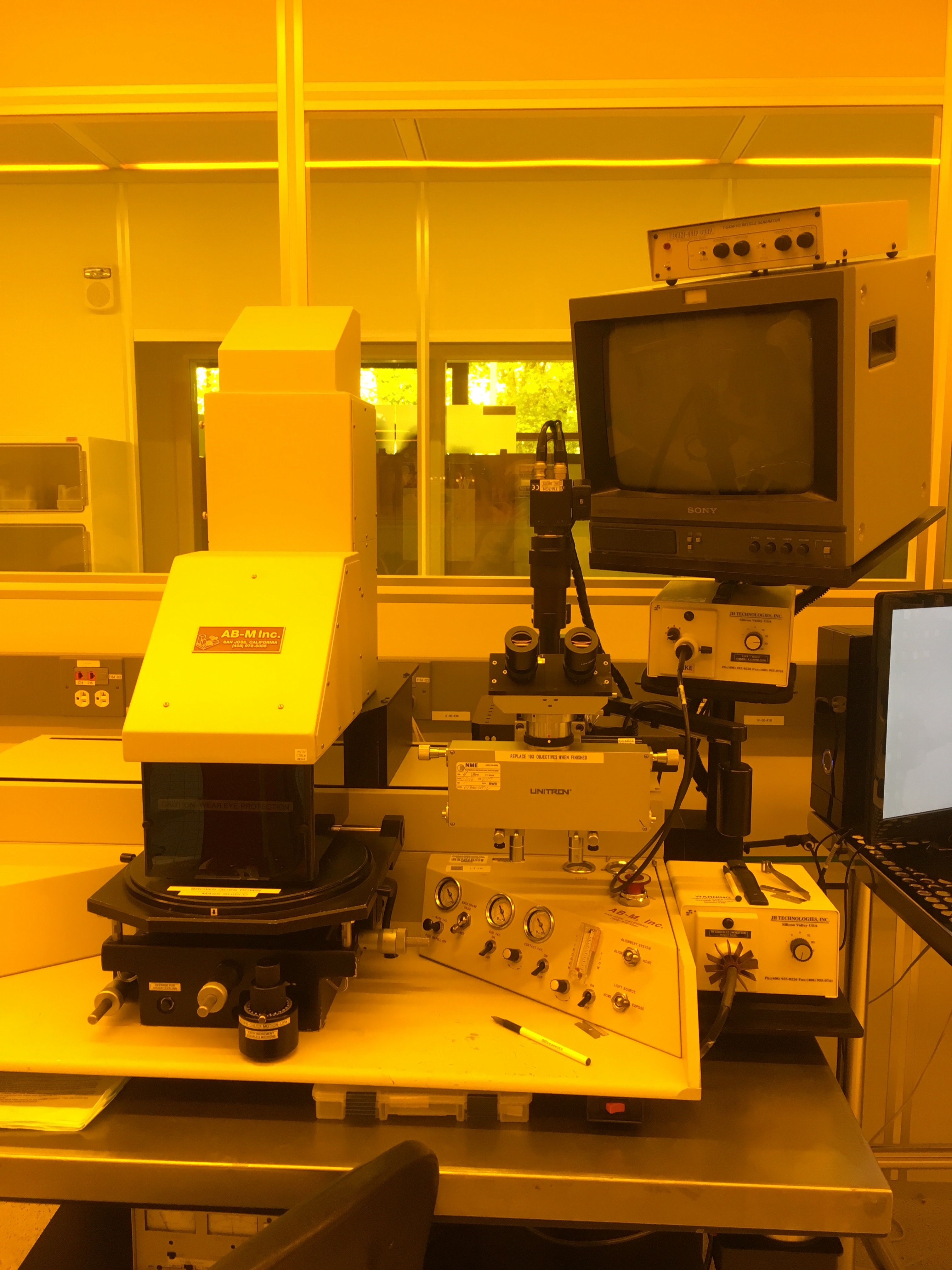
ABM Contact Aligner
| Coral ID: | WNF--Aligner--ABM |
| Manufacturer: | AB-M |
| Lab: | WNF |
| Area: | Lithography and Direct Patterning |
| Manual: | https://www.coral.washington.edu/upload/manuals/ABM SOP (Teaching Lab).pdf |
| UW Academic Rate: | $55/hr |
| Industrial Rate: | $165/hr |
| Outside Academic Rate: | $55/hr |
Description
Contact photolithography exposure tool for 100mm wafers. An optimized process can achieve 2 um line/space patterns with a layer-to-layer registration accuracy about 3 um.
Details
(none given)
Materials Restrictions
Uses 5in or 7in square photomasks with 0.090in thickness. Configured for exposure of 100mm wafers; smaller chips can be accomodated using a carrier wafer.
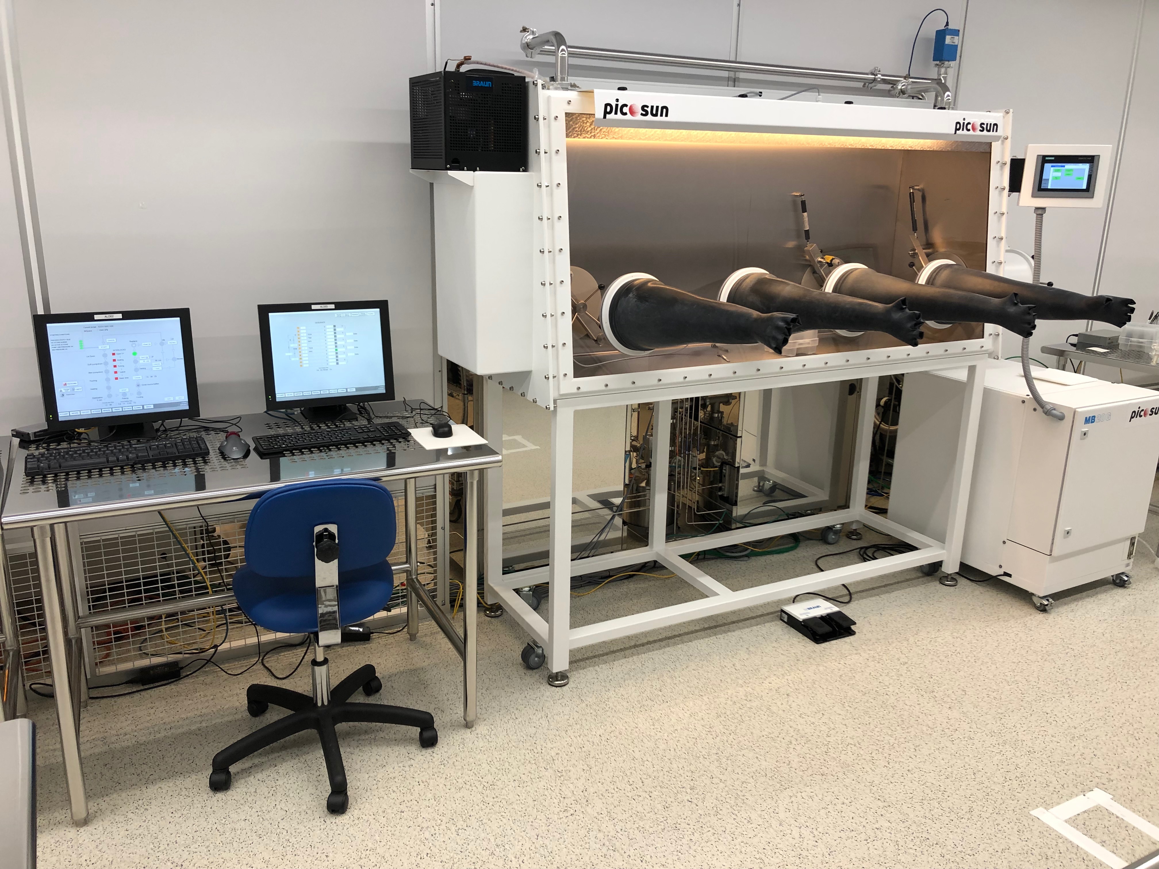
ALD chamber
| Coral ID: | WNF--ALD02--Picosun-R200 |
| Manufacturer: | Picosun |
| Model: | R200 |
| Lab: | WNF |
| Area: | Thin Film Processing |
| Manual: | https://www.coral.washington.edu/upload/manuals/ALD02 and ALD03 SOP 20240229.pdf |
| UW Academic Rate: | $33/hr |
| Industrial Rate: | $99/hr |
| Outside Academic Rate: | $33/hr |
Description
Picosun tool number 400309
MBraun glove box project #11939
Details
Existing processes: Al2O3, AlN, SiO2, ZrO2
Other processes available on request: HfO2, ZnO
Chips, 1 to 25 100mm wafers, 1 to 6 150mm wafers, or single 200mm wafer per run.
TDMACZ - tris(dimethylamino)cyclopentadienyl zirconium
BDEAS - bis(diethylamino)silane
TMA - trimethyl aluminum
TEMAH - tetrakis(ethylmethylamino) hafnium
Materials Restrictions
(none)
ALD chamber
| Coral ID: | WNF--ALD03--Picosun-R200 |
| Manufacturer: | Picosun |
| Model: | R200 |
| Lab: | WNF |
| Area: | Thin Film Processing |
| Manual: | https://www.coral.washington.edu/upload/manuals/ALD02 and ALD03 SOP 20240229.pdf |
| UW Academic Rate: | $33/hr |
| Industrial Rate: | $99/hr |
| Outside Academic Rate: | $33/hr |
Description
Picosun tool number 400310
MBraun glove box project #11939
Details
Existing processes: Al2O3, AlN, Pt, TiO2, TiN, TiO2
Other processes available on request: Ru
Chips, 1 to 25 100mm wafers, 1 to 6 150mm wafers, or single 200mm wafer per run.
Me3(MeCp)Pt - trimethyl(methylcyclopentadienyl) platinum
(EtCp)2Ru - bis(ethylcyclopentadienyl) ruthenium
TDMAT - tetrakis(dimethylamino) titanium
TMA - trimethyl aluminum
Materials Restrictions
(none)
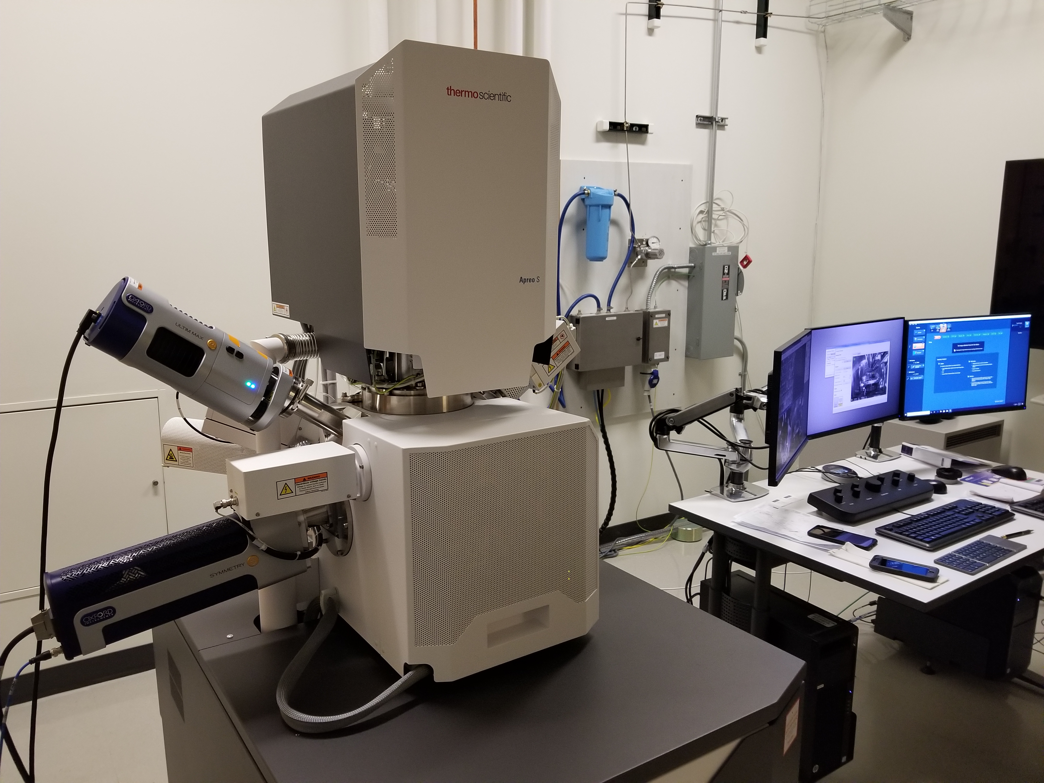
Apreo Variable Pressure SEM
| Coral ID: | MAF--SEM--Thermo-Apreo-S |
| Manufacturer: | ThermoFisher Scientific |
| Model: | Apreo S |
| Lab: | MAF |
| Area: | Inspection |
| Manual: | https://www.coral.washington.edu/upload/manuals/Apreo User Operational Manual 1st Edition.pdf |
| UW Academic Rate: | $55/hr |
| Industrial Rate: | $200/hr |
| Outside Academic Rate: | $64/hr |
Description
The TFS Apreo variable-pressure SEM is a hi-resolution SEM capable of 1nm resolution and excellent back-scatter contrast.
Details
Standard ETD in-chamber SE detector, T1 BSE detector and T2 in-column SE detector. Optionally equipped with immersion mode and T3 in-column SE detector, retractable directional back-scatter detector (DBS) with concentric and angular diode arrangements (available up to 50Pa chamber pressure), and sTEM 3+ transmission electron detector with concentric diodes for HAADF, BF, and custom DF imaging. Sample stage tilts to 90-deg. Variable pressure sample chamber can maintain 10-500 Pa water-vapor environment or high vacuum (10e-4 Pa). Has Maps4 automated large area mapping software. Equipped with Oxford Symmetry (EBSD) with EDS.
Materials Restrictions
Up to 110mm long and 50mm tall. Vacuum compatible to 10e-4 Pa
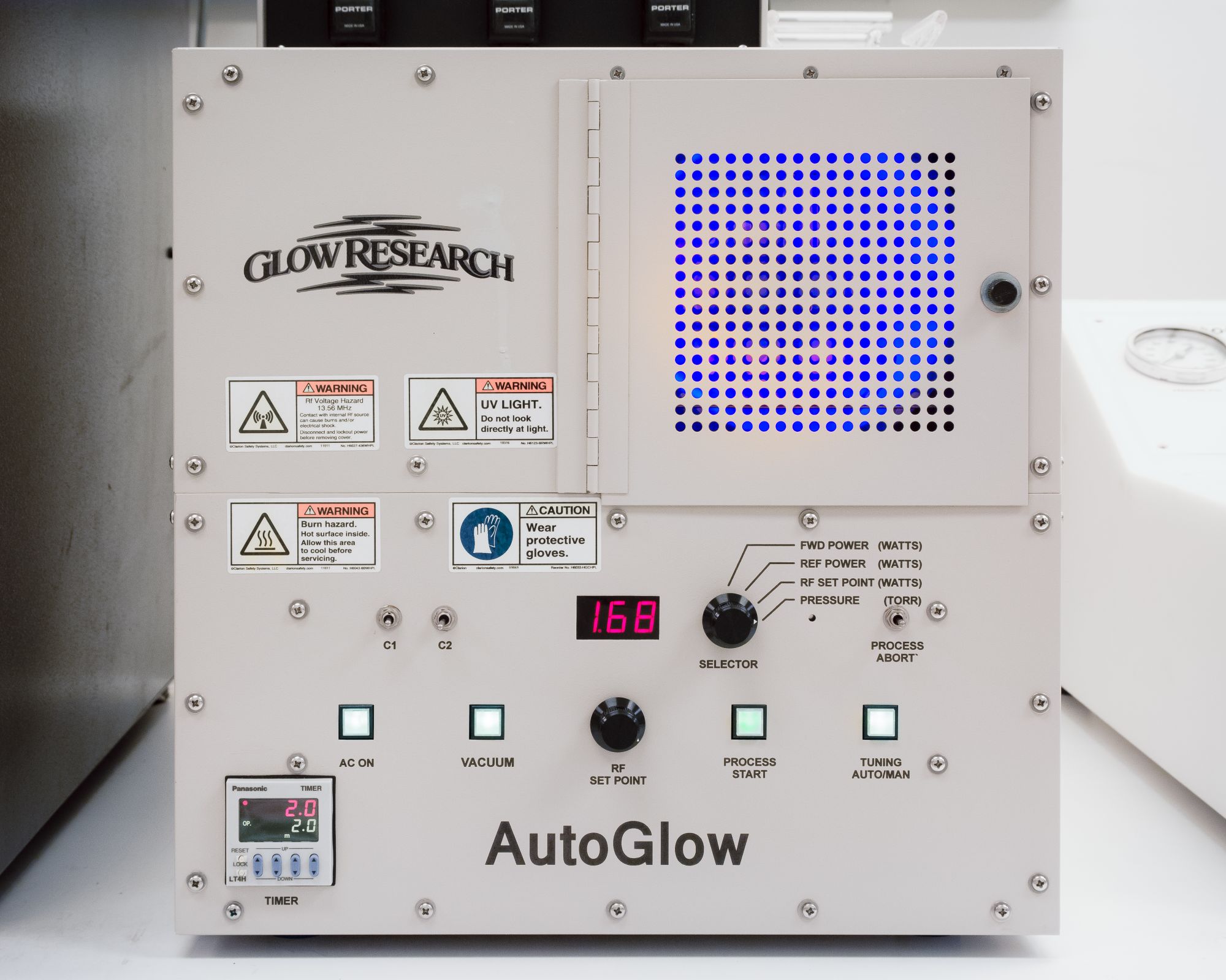
Barrel Asher
| Coral ID: | WNF--Asher--BarrelEtch |
| Manufacturer: | Glow Research |
| Model: | AutoGlow |
| Lab: | WNF |
| Area: | Lithography and Direct Patterning |
| Manual: | https://www.coral.washington.edu/upload/manuals/SOP_Barrel_Asher_v2d.pdf |
| UW Academic Rate: | $55/hr |
| Industrial Rate: | $165/hr |
| Outside Academic Rate: | $55/hr |
Description
Barrel asher used to strip resist or other organic films, descum patterned resist, or clean surfaces of residual organics using an isotropic oxygen plasma.
Details
Accomodates substrate from chips up to 100mm diameter wafers.
Materials Restrictions
Allowed etch target materials: Photoresist, e-beam resist, organic contaminants, other polymers (No SU8 nor PDMS.) No high-vapor-pressure materials. Please contact tool owner to discuss materials not included on this list.
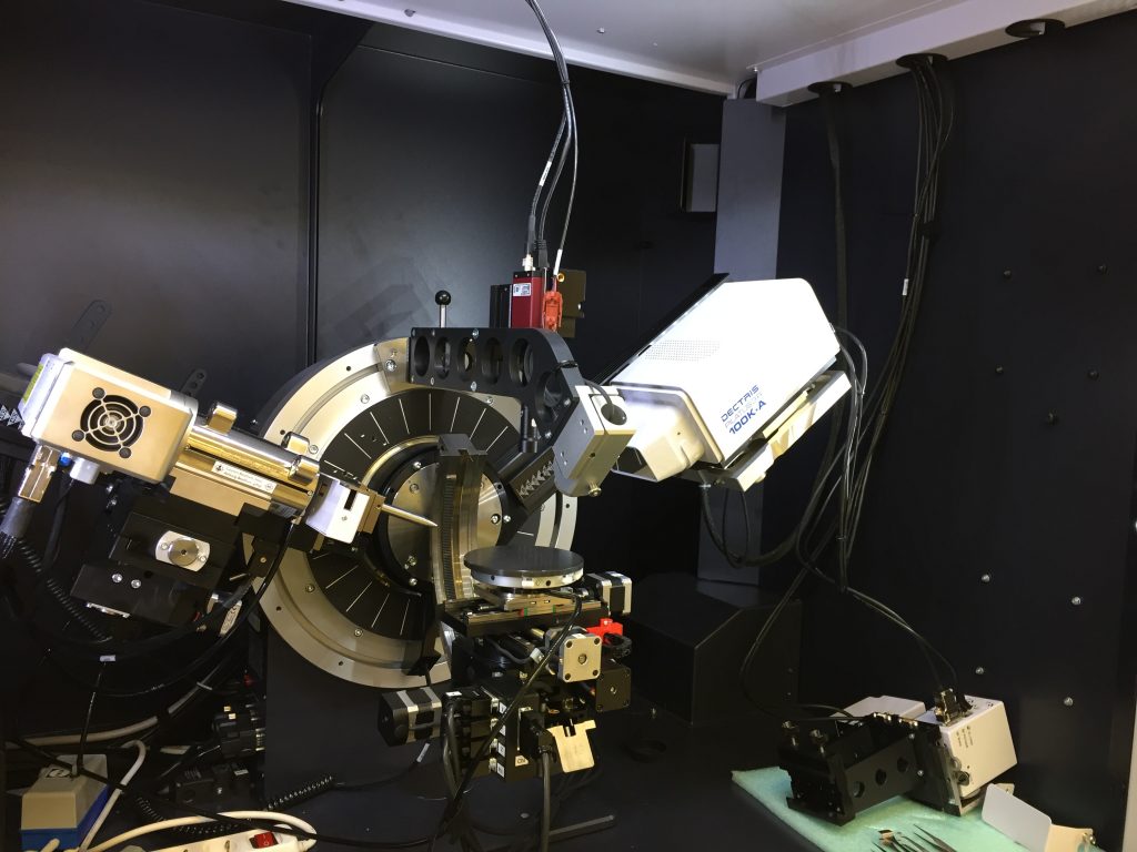
Bruker D8 Discover with IμS 2-D XRD System
| Coral ID: | MAF--XRD--Bruker-Microfocus |
| Manufacturer: | Bruker |
| Model: | D8 Discover Microfocus |
| Lab: | MAF |
| Area: | Device and Structure Characterization |
| Manual: | https://www.coral.washington.edu/upload/manuals/Bruker D8 microfocus SOP_December 2022.pdf |
| UW Academic Rate: | $55/hr |
| Industrial Rate: | $200/hr |
| Outside Academic Rate: | $64/hr |
Description
By combining a high-efficiency Cu anode microfocus x-ray source and an extremely sensitive Pilatus 100K large-area 2D detector, the Bruker D8 powder x-ray diffractometer delivers some of the shortest acquisition times available. Additionally the 2D detection system gives unique information such as film orientation and strain, not easily achievable with traditional powder diffractometers. Since the instrument operates in a collimated beam geometry (0.05-2 mm beam diameter), only a very small amount of sample is necessary (less than 1 mg), and good diffraction can be collected from non-flat surfaces. The Pilatus 100K is capable of suppressing fluorescence from most samples (eg those containing Fe), and is not damaged by being hit with the main beam. This allows SAXS measurements without a beamstop. Phase Identification, Phase Quantification (or % crystallinity), Texture, Stress, High Throughput Screening, MicroDiffraction, Mapping and more can be done faster and more easily on this system. The system also can be used with a Lynxeye-XET multi-strip 1D detector. This allows for higher resolution, Rietveld quality data collection, and x-ray reflectivity (XRR) measurements. A temperature controlled sample stage is also available for measurements from -100 to 350 °C with the sample in vacuum atmosphere.
Details
(none given)
Materials Restrictions
(none)
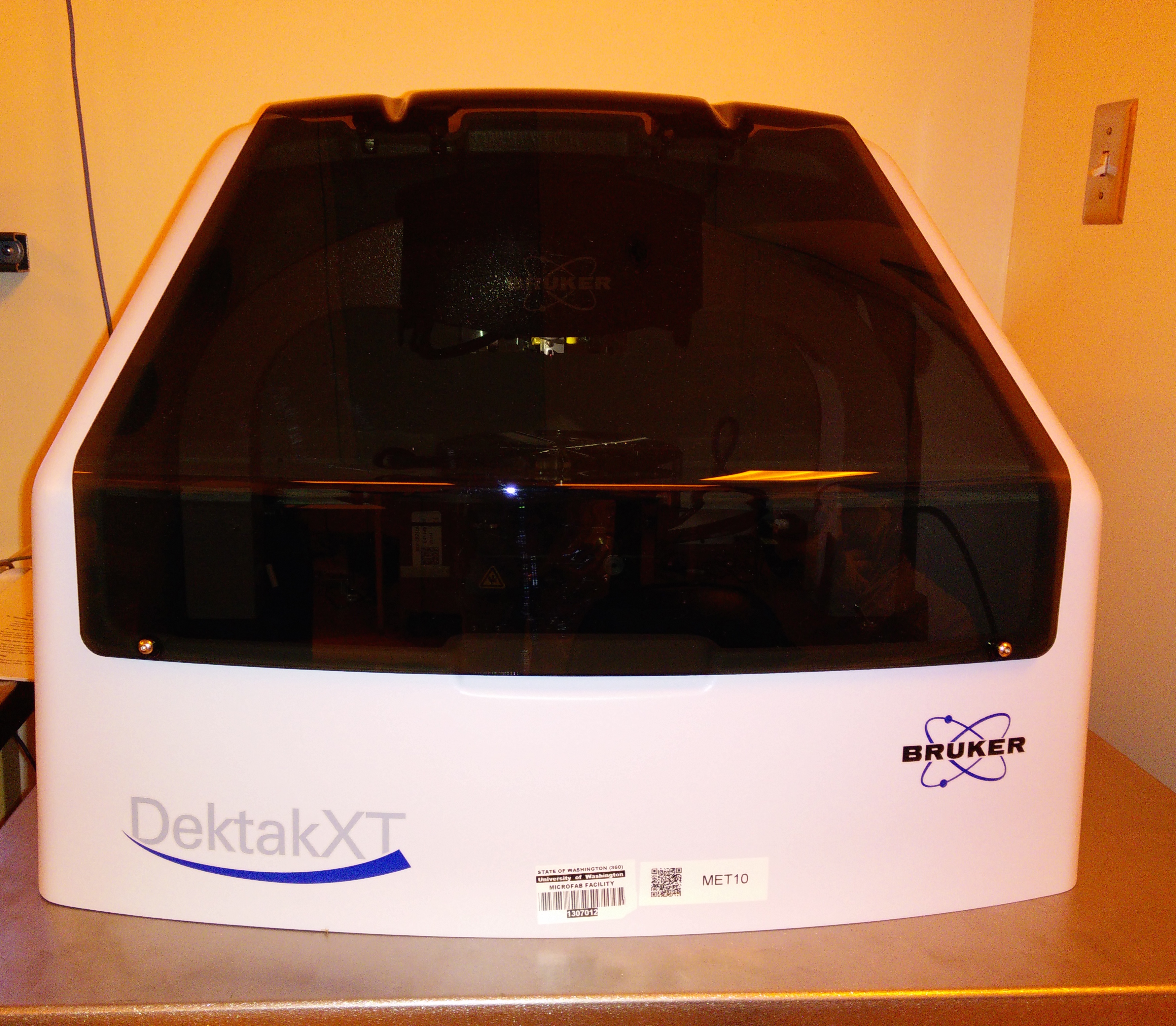
Bruker DektakXT Contact Profilometer
| Coral ID: | WNF--Profilometer--Dektak-XT |
| Manufacturer: | Bruker |
| Model: | WNF--Profilometer--Dektak-XT |
| Lab: | WNF |
| Area: | Device and Structure Characterization |
| Manual: | https://www.coral.washington.edu/upload/manuals/DektakXT SOP 20190523 Full.pdf |
| UW Academic Rate: | $55/hr |
| Industrial Rate: | $165/hr |
| Outside Academic Rate: | $55/hr |
Description
This is a contact profilometer capable of measuring step heights that range from tens of nanometers to one millimeter. It can also measure surface roughness and film stress. It can accommodate 100mm, 125 mm, and 150 mm wafers as well as smaller chips. It is capable of automated measurements with step detection. The stylus has a radius of 2 um and a cone angle of 60 degrees.
Details
(none given)
Materials Restrictions
(none)
capillary Differential Scanning Calorimeter
| Coral ID: | MAF--Calorimeter--capDSC |
| Lab: | MAF |
| Area: | Biological/Chemical/Particle Technology |
| UW Academic Rate: | $22/hr |
| Industrial Rate: | $126/hr |
| Outside Academic Rate: | $26/hr |
Description
Measurment of domain stability, melting temperature, and total thermodynamic determination of protein unfolding
Details
MicroCal cap DSC liquid samples only volumes 400uL
Materials Restrictions
(none)
Cascade Microtech M150
| Coral ID: | WNF--ProbeStation |
| Manufacturer: | Cascade Microtech |
| Model: | M150 |
| Lab: | WNF |
| Area: | Packaging and Back End |
| UW Academic Rate: | $33/hr |
| Industrial Rate: | $99/hr |
| Outside Academic Rate: | $33/hr |
Description
This manual probe station is typically used to measure conductivity, IV curves, and capacitance. It can be configured for many measurements and has a camera capable of recording video of moving MEMS devices.
Details
(none given)
Materials Restrictions
(none)
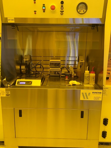
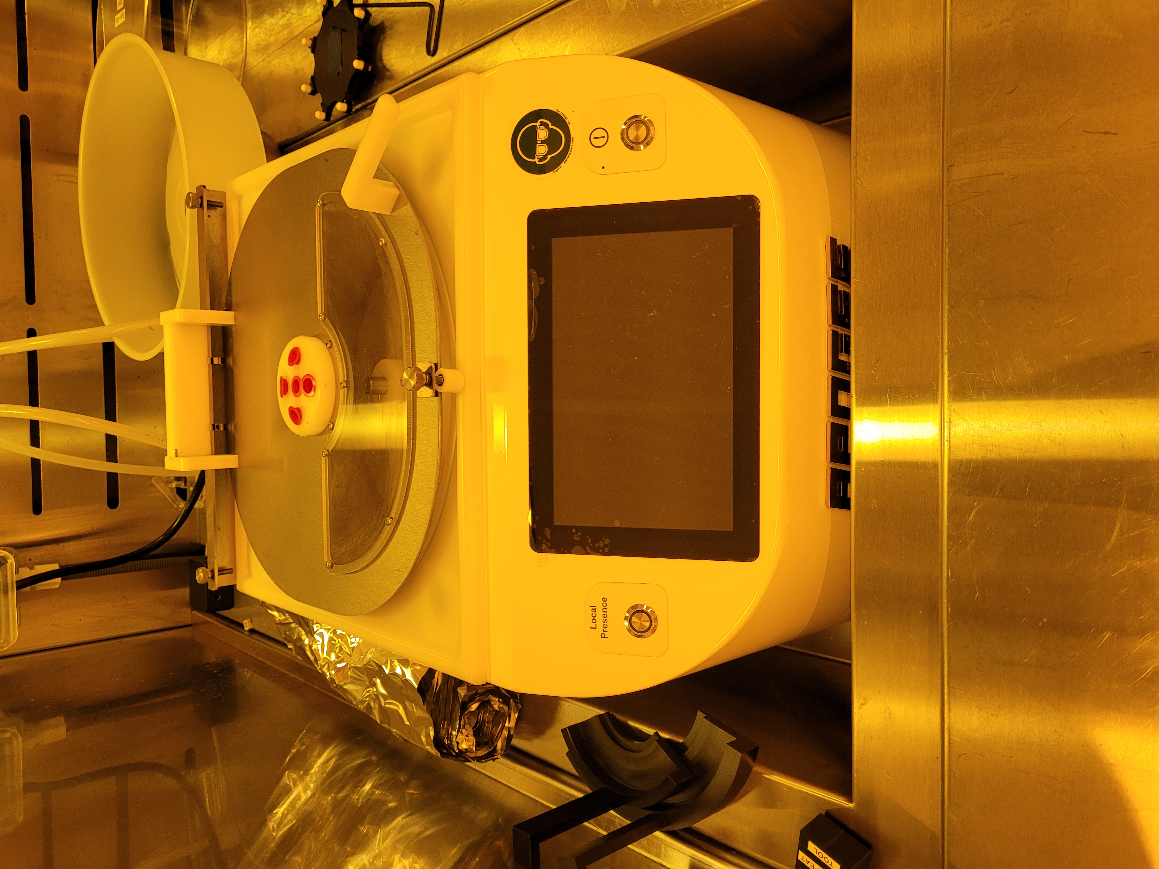
CEE Apogee Spin Coater
| Coral ID: | WNF--SPIN5 |
| Manufacturer: | WAFAB |
| Model: | 48" SST Front Acess Wet Bench |
| Lab: | WNF |
| Area: | Lithography and Direct Patterning |
| Manual: | https://www.coral.washington.edu/upload/manuals/SPIN4_5_Apogee_SOP_V1.2.pdf |
| UW Academic Rate: | $55/hr |
| Industrial Rate: | $165/hr |
| Outside Academic Rate: | $55/hr |
Description
Flexible, manual bench-top spin coater with vacuum chucks available for pieces from a few mm up to 150 mm wafers.
Details
(none given)
Materials Restrictions
(none)
CO2 Laser
| Coral ID: | WNF--LaserCutter--M20 |
| Manufacturer: | Universal Laser |
| Model: | M20 |
| Lab: | WNF |
| Area: | Packaging and Back End |
| UW Academic Rate: | $33/hr |
| Industrial Rate: | $99/hr |
| Outside Academic Rate: | $33/hr |
Description
Laser cutting of polymer films.
Details
(none given)
Materials Restrictions
(none)
Critical Point Drier
| Coral ID: | MAF--CPD--Tousimis-SamDri-780 |
| Manufacturer: | Tousimis |
| Model: | SamDri-780 |
| Lab: | MAF |
| Area: | Other |
| UW Academic Rate: | $0/hr |
| Industrial Rate: | $0/hr |
| Outside Academic Rate: | $0/hr |
Description
Instrument that performs dehydration of biological tissue or other hydrated materials prior to high-vacuum SEM characterization. Ethanol in the sample is exchanged for liquid CO2 then the vessel is heated under pressure beyond the CO2 critical point (1100psi at 32C). A typical sample of cells on coverglass requires about 90 minutes to properly dry. Solid tissues can take significantly longer.
Details
Chamber is a vertical cylinder 2.9cm diameter and 9cm tall.
Materials Restrictions
(none)
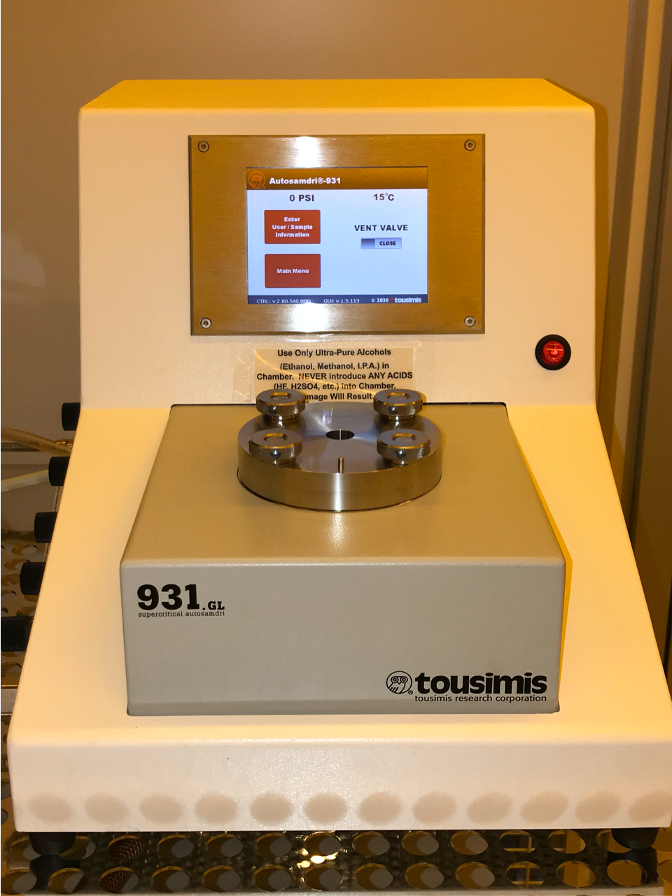
Critical Point Dryer
| Coral ID: | WNF--CPD01-Tousimis |
| Manufacturer: | Tousimis |
| Model: | 931 |
| Lab: | WNF |
| Area: | Wet Etch and Cleaning |
| Manual: | https://www.coral.washington.edu/upload/manuals/CPD_SOP_20210517.pdf |
| UW Academic Rate: | $11/hr |
| Industrial Rate: | $33/hr |
| Outside Academic Rate: | $11/hr |
Description
The Tousimis Critical Point Dryer (CPD) uses liquid carbon dioxide (LCO2) to dry and release fragile parts without damaging the structure due to surface tension.
Details
(none given)
Materials Restrictions
(none)
Dektak Profilometer
| Coral ID: | MAF--Profilometer--Bruker-DektakXT |
| Manufacturer: | Bruker |
| Model: | OM-DektakXT |
| Lab: | MAF |
| Area: | Thin Film and Materials Characterization |
| UW Academic Rate: | $22/hr |
| Industrial Rate: | $126/hr |
| Outside Academic Rate: | $26/hr |
Description
Profilometer for measuring sub-nanoscale to millimeter scale film thicknesses, roughness, and thin film tensile and compressive stressed.
Details
Diamond stylus with 2 um radius.
Materials Restrictions
(none)
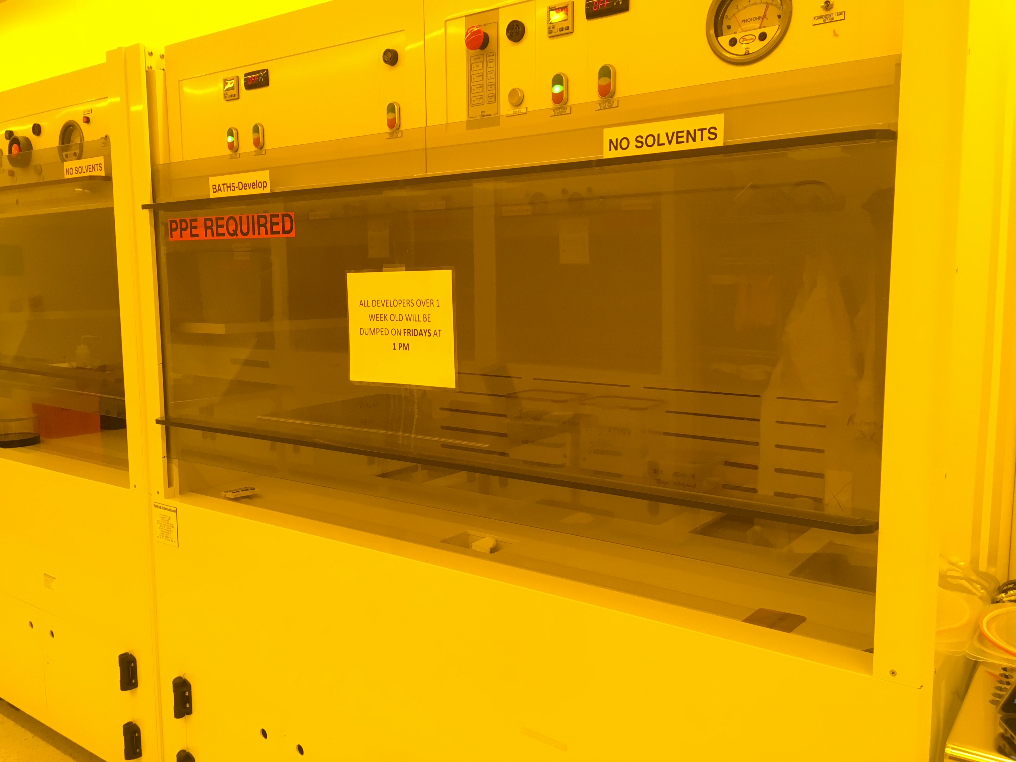
Developer Station
| Coral ID: | WNF--BATH5-Develop |
| Manufacturer: | WAFAB International |
| Model: | 72" PVC-C Front Access Wet Bench (Developer Station) |
| Lab: | WNF |
| Area: | Wet Etch and Cleaning |
| Manual: | https://www.coral.washington.edu/upload/manuals/BATH5-Develop_3.0.pdf |
Description
Wet bench with dedicated baths for photoresist developers
Details
(none given)
Materials Restrictions
(none)
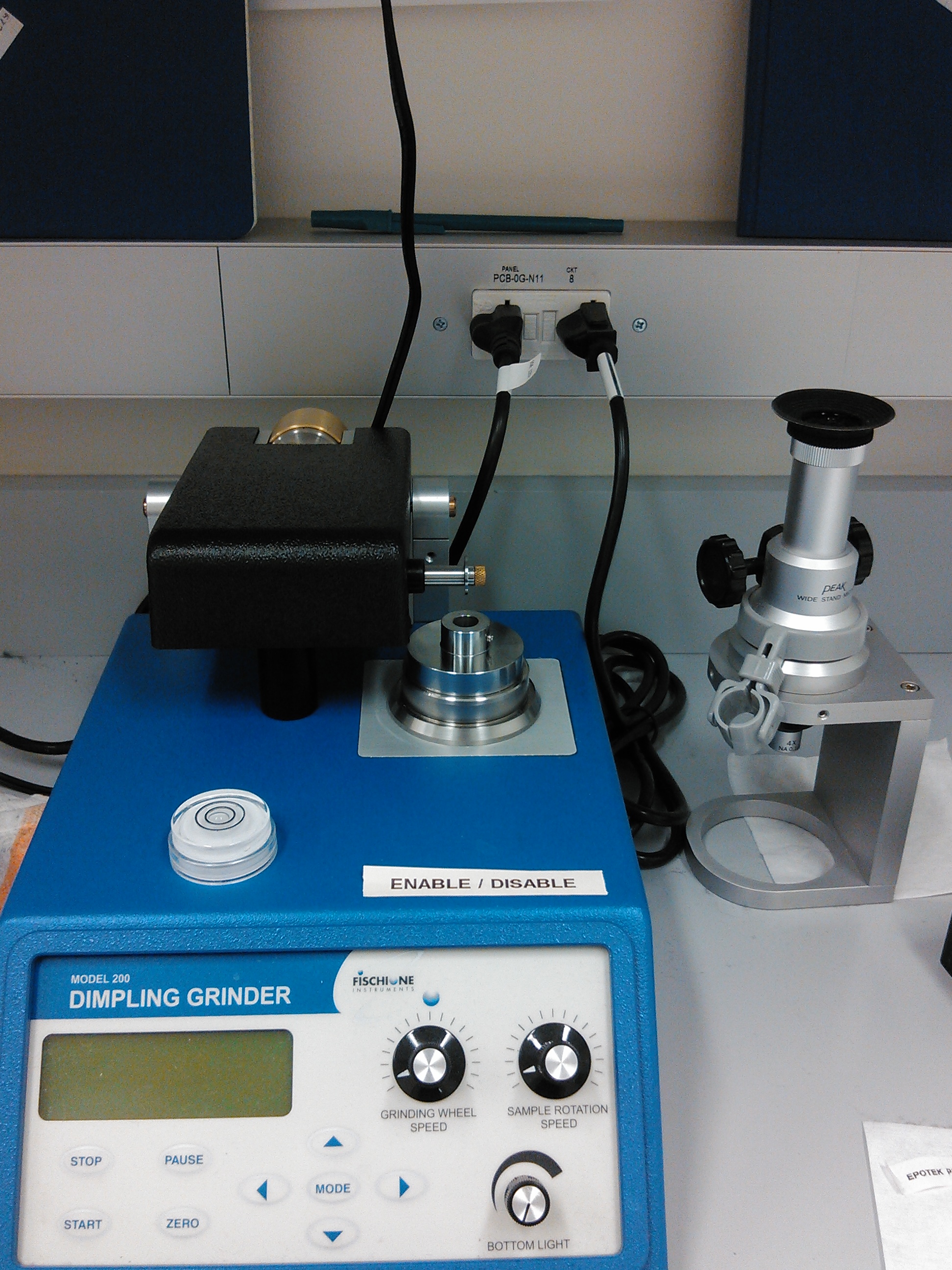
Dimple Grinder
| Coral ID: | MAF--Dimple-Grinder--Fischione-200 |
| Manufacturer: | Fischione |
| Model: | 200 |
| Lab: | MAF |
| UW Academic Rate: | $34/hr |
| Industrial Rate: | $126/hr |
| Outside Academic Rate: | $40/hr |
Description
The Fischione Dimple Grinder is an intermediate step in the preparation of hard (conventional) materials for TEM analysis. Dimple grinding follows planarization and polish and precedes ion-milling.
Details
Capable of both 1-sided and double-sided dimple grinding with 1um resolution.
Materials Restrictions
Contact staff to inquire about the suitability to your material.
Disco Wafer Backgrinder
| Coral ID: | WNF--Grinder--Disco |
| Manufacturer: | Disco America |
| Model: | DAG810 |
| Lab: | WNF |
| Area: | Packaging and Back End |
| Manual: | https://www.coral.washington.edu/upload/manuals/DAG810_SOP1.1.pdf |
| UW Academic Rate: | $77/hr |
| Industrial Rate: | $231/hr |
| Outside Academic Rate: | $77/hr |
Description
Wafer backgrinder capable of bulk grinding and thinning of 200mm diameter wafers and smaller, including chips.
Details
(none given)
Materials Restrictions
No metals; wastestream safe materials only
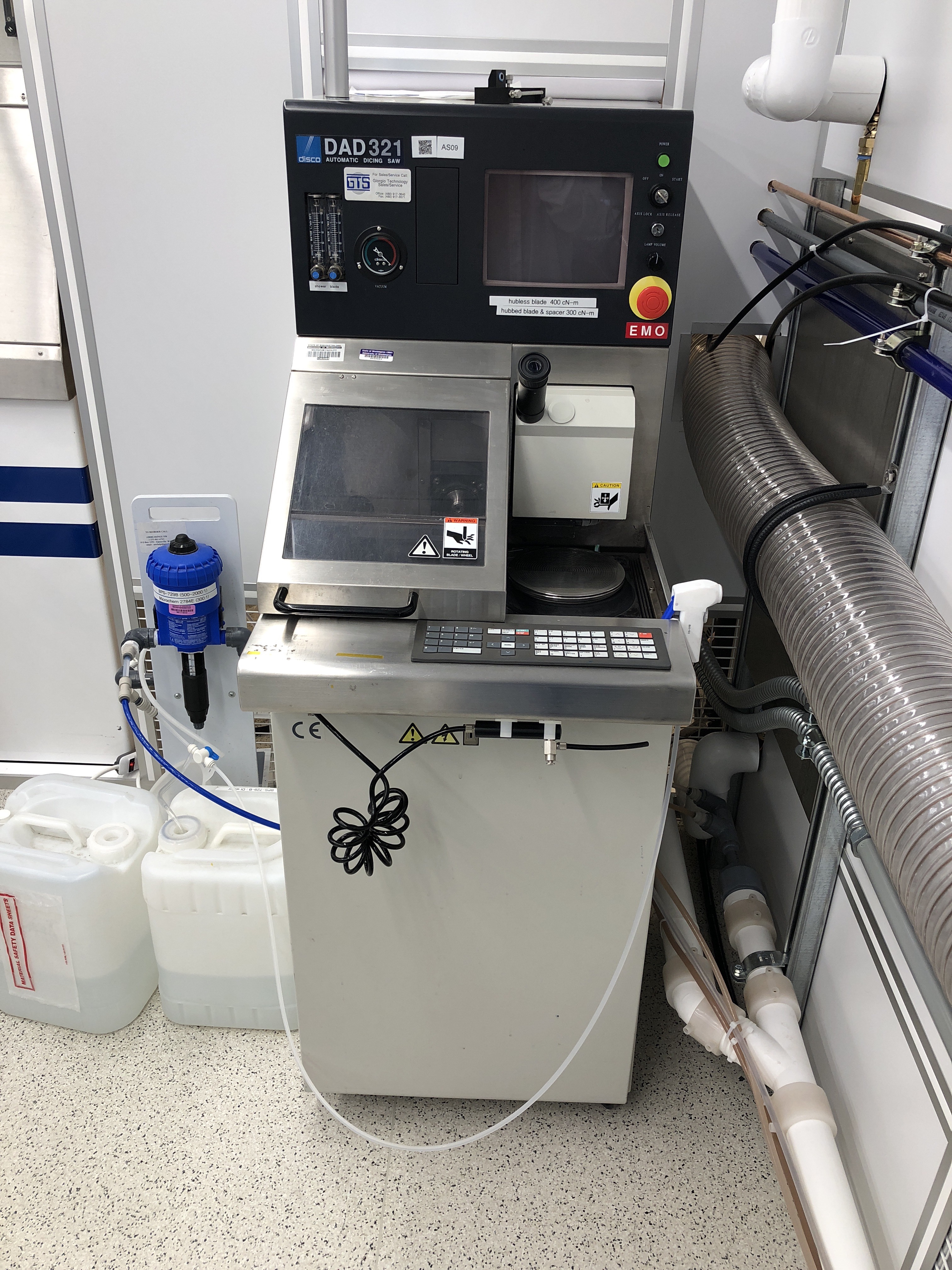
Disco Wafer Dicer
| Coral ID: | WNF--Saw--Disco |
| Manufacturer: | Disco America |
| Model: | DAD321 |
| Lab: | WNF |
| Area: | Packaging and Back End |
| Manual: | https://www.coral.washington.edu/upload/manuals/DiscoDAD SOP 3.2.pdf |
| UW Academic Rate: | $55/hr |
| Industrial Rate: | $165/hr |
| Outside Academic Rate: | $55/hr |
Description
Wafer dicing capable of 150mm diameter wafers and smaller.
Details
(none given)
Materials Restrictions
Silicon, glass, sapphire, other semiconductors crystalline structures. No bulk metal dicing; stack materials must be wastestream safe.
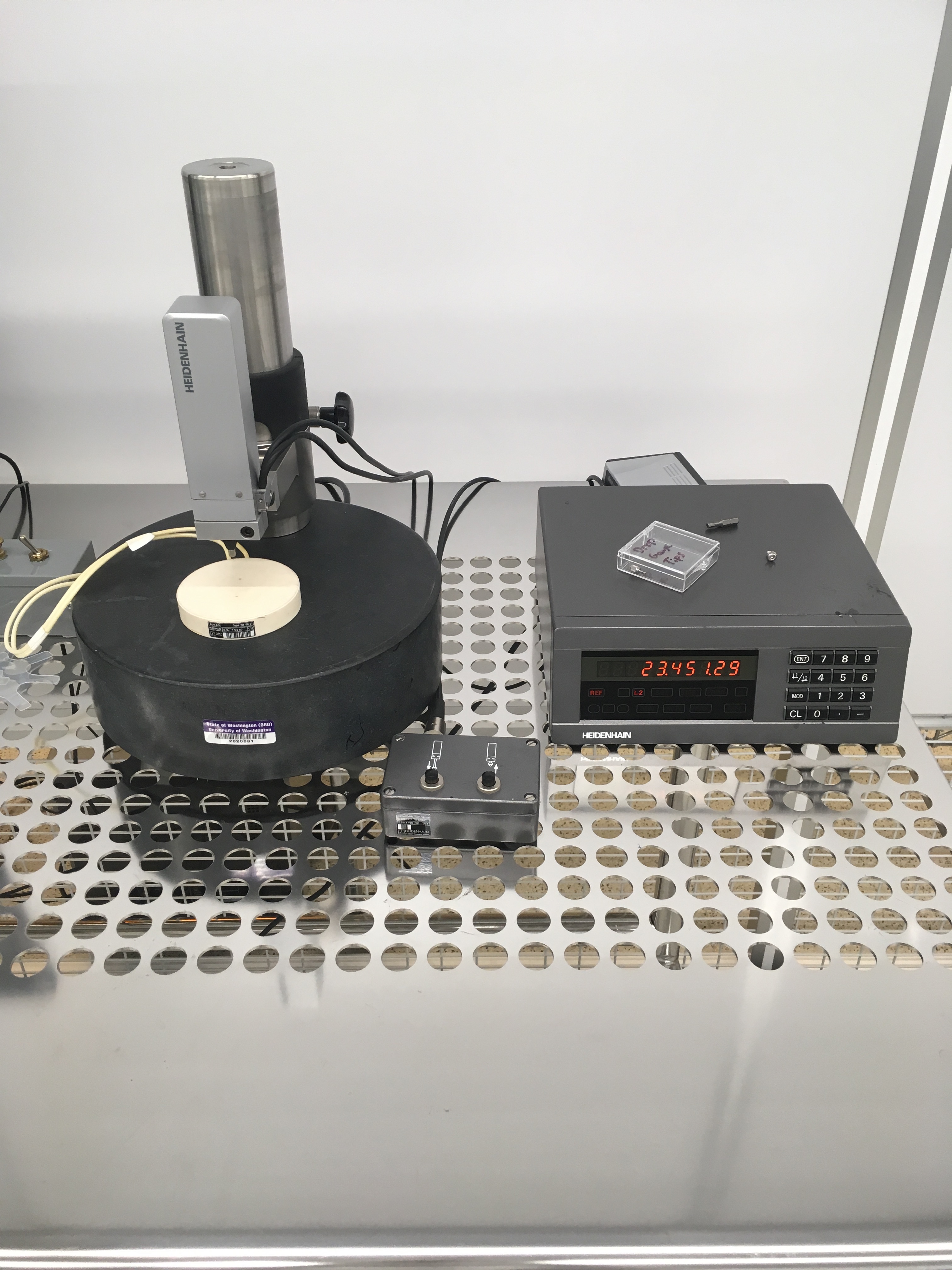
Drop Gauge
| Coral ID: | WNF--DropGauge |
| Manufacturer: | HEIDENHAIN |
| Model: | ND 281A |
| Lab: | WNF |
| Area: | Thin Film and Materials Characterization |
| Manual: | https://www.coral.washington.edu/upload/manuals/DropGauge SOP 1.0.pdf |
| UW Academic Rate: | $0/hr |
| Industrial Rate: | $0/hr |
| Outside Academic Rate: | $0/hr |
Description
The drop gauge is a quick way to measure thickness of a sample. It has a range of 25 mm and an accuracy of 0.1 �m. The system consists of a measuring probe, a vacuum chuck, motion control box, and a numerical display box for measurement readout.
Details
(none given)
Materials Restrictions
- Ensure substrates are clean and dry
- The measurement probe will press into soft materials, causing inaccuracy in measurements and potentially damage to sensitive features. Choose measurement area accordingly.
Dual beam UV/vis
| Coral ID: | MAF--Spectrophotometer--Evolution-220 |
| Manufacturer: | Thermofihser |
| Model: | Evolution 220 |
| Lab: | MAF |
| Area: | Biological/Chemical/Particle Technology |
| UW Academic Rate: | $6/hr |
| Industrial Rate: | $17/hr |
| Outside Academic Rate: | $7/hr |
Description
Dual beam UV/vis spectrophotometer, photodiode array detector, no thermal control
Details
(none given)
Materials Restrictions
(none)
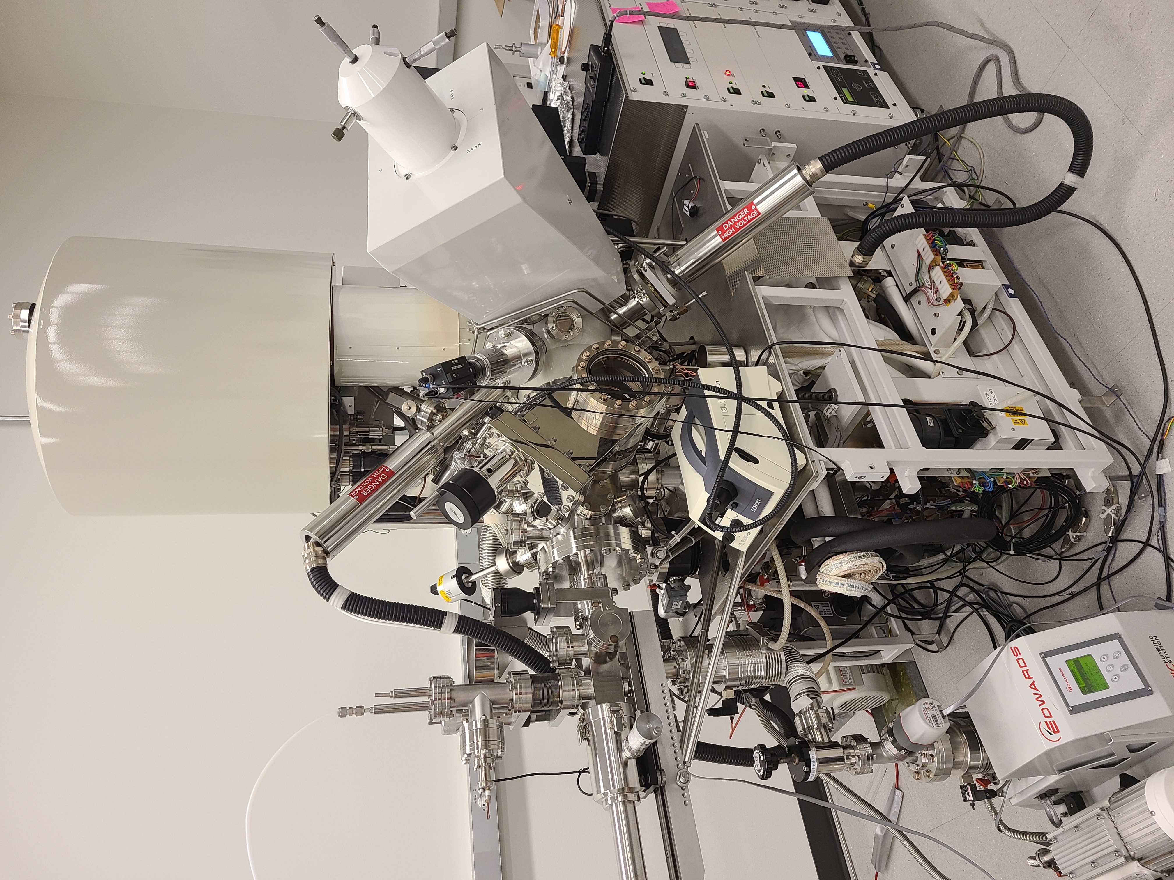
Dualbeam FIB-SEM
| Coral ID: | MAF--Dual-Beam-SEM-FIB--FEI-XL830 |
| Manufacturer: | FEI |
| Model: | XL830 |
| Lab: | MAF |
| Area: | Inspection |
| Manual: | https://www.coral.washington.edu/upload/manuals/DualBeamManual_v0915.pdf |
| UW Academic Rate: | $55/hr |
| Industrial Rate: | $200/hr |
| Outside Academic Rate: | $64/hr |
Description
FEI XL830 dual-beam SEM-FIB is a single platform for both hi-resolution electron/ion imaging and site specific milling for a variety of applications. The electron beam allows observation of samples while the FIB accomplishes nano-machining of samples and devices for device editing, failure analysis, and sublayer observation.
Details
Equipped with a field-emission SEM column (res~4nm) and a gallium focused ion beam (FIB). Detectors include Through Lens Detector (TLD), sTEM, and Continuous Dynode Electron Multiplier (CDEM) for secondary electron, backscattered electron, and secondary ion imaging. A stationary microprobe is available in the chamber for extraction of TEM lamella from wafer substrates. Beam chemistries include enhanced Si/SiOx etch and site specific platinum deposition.
Materials Restrictions
Samples must be conductive and vacuum safe to 10^-8 mTorr. Chamber will accommodate an 6" wafer or multiple smaller pin-mount stubs. Mounted sample height must be below 8mm.
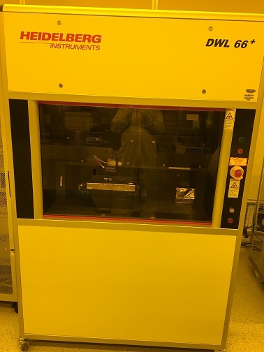
DWL66+ Direct Write
| Coral ID: | WNF--MaskWriter--Heidelberg-DWL66plus |
| Manufacturer: | Heidelberg |
| Model: | DWL66+ |
| Lab: | WNF |
| Area: | Lithography and Direct Patterning |
| Manual: | https://www.coral.washington.edu/upload/manuals/DWL66+Basic_032022.pdf |
| UW Academic Rate: | $33/hr |
| Industrial Rate: | $99/hr |
| Outside Academic Rate: | $33/hr |
Description
Create masks or direct write on substrates with alignment capability utilizing a 405nm laser. Write modes HiRes with 300nm minimum feature, 4mm head with 0.8um minimum feature, and 20mm head with 2um minimum feature.
Details
(none given)
Materials Restrictions
(none)
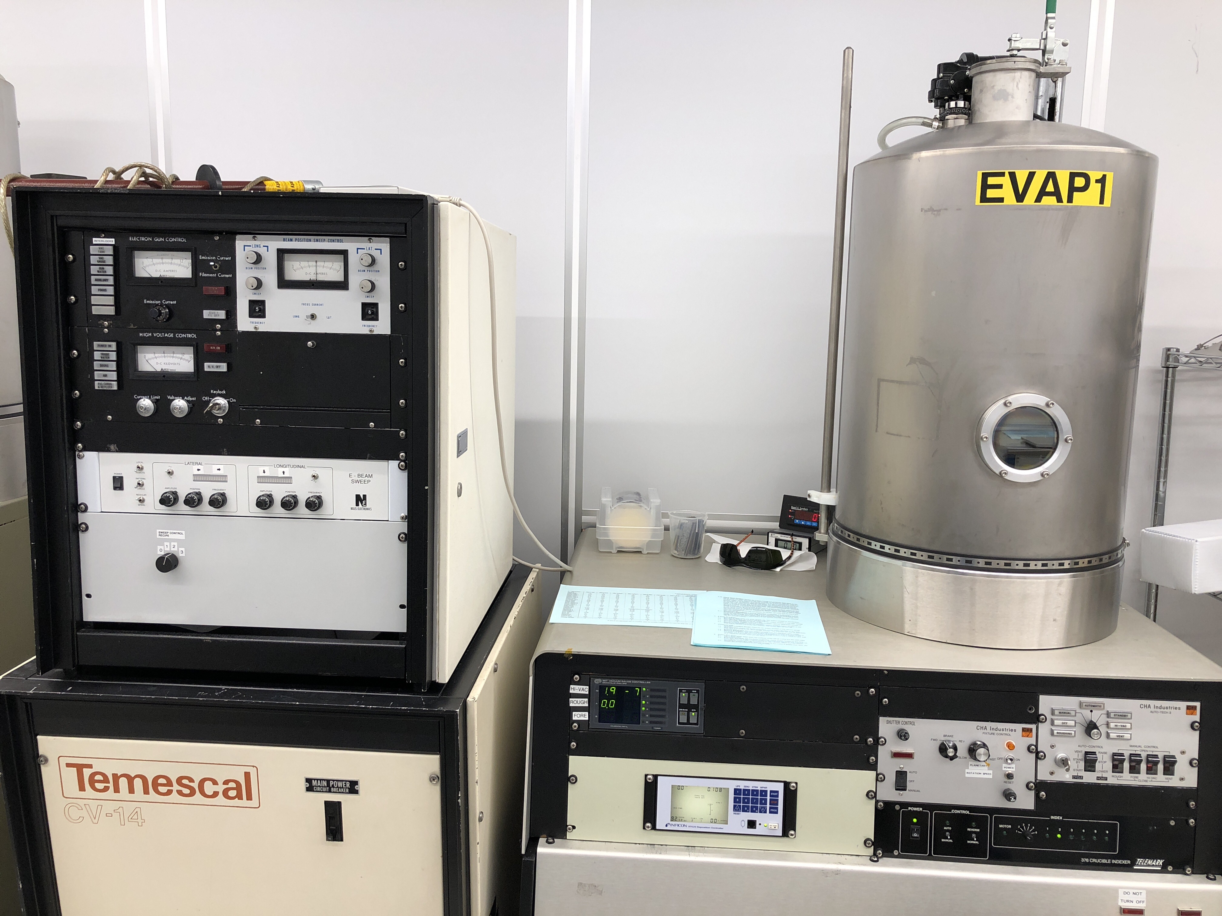
E-beam Evaporator 1
| Coral ID: | WNF--EVAP1 |
| Manufacturer: | CHA |
| Model: | SEC-600 |
| Lab: | WNF |
| Area: | Thin Film Processing |
| Manual: | https://www.coral.washington.edu/upload/manuals/EVAP1 - SOP.pdf |
| UW Academic Rate: | $77/hr |
| Industrial Rate: | $231/hr |
| Outside Academic Rate: | $77/hr |
Description
EVAP1 is an electron beam evaporator for depositing metal films. It is cryopumped with a base pressure less than 2x10⁻⁶ Torr. The system holds 4 crucibles of metal, thus up to 4 metals can be subsequently deposited.
Details
The system has a capacity up to nine 100mm wafers in a planetary holder. Smaller pieces can be held by inserts. Typical evaporation sources are Ti, Au, Cr, Pt, Ag, Al, Pd, Cu, and Ni. Other sources are available. Precious metals (Au, Pt, and Pd) are charged by use. Users are welcome to request new materials and need to work with staff on developing proper recipes. The distance from the evaporation source to the wafer holder is about 19.5 inches.
Serial Number: 11199
Gold, palladium, and platinum must be weighed before and after use. A scale for this is available next to the checkout sheet. Make sure the gold crucible is placed on two carbon disks. The platinum crucible must make very good thermal contact with the hearth to avoid melting. Make sure the crucible fits all the way into the hearth with the top of the crucible flush with the hearth, and that the hearth is very clean before it is loaded.
Materials Restrictions
Only pure metals are recommended. The evaporation process typically does not allow for effective deposition of compound materials. Photoresist-coated substrates are allowed. Inorganic substrates are allowed in the system. Organic substrates may be allowed with staff permission.
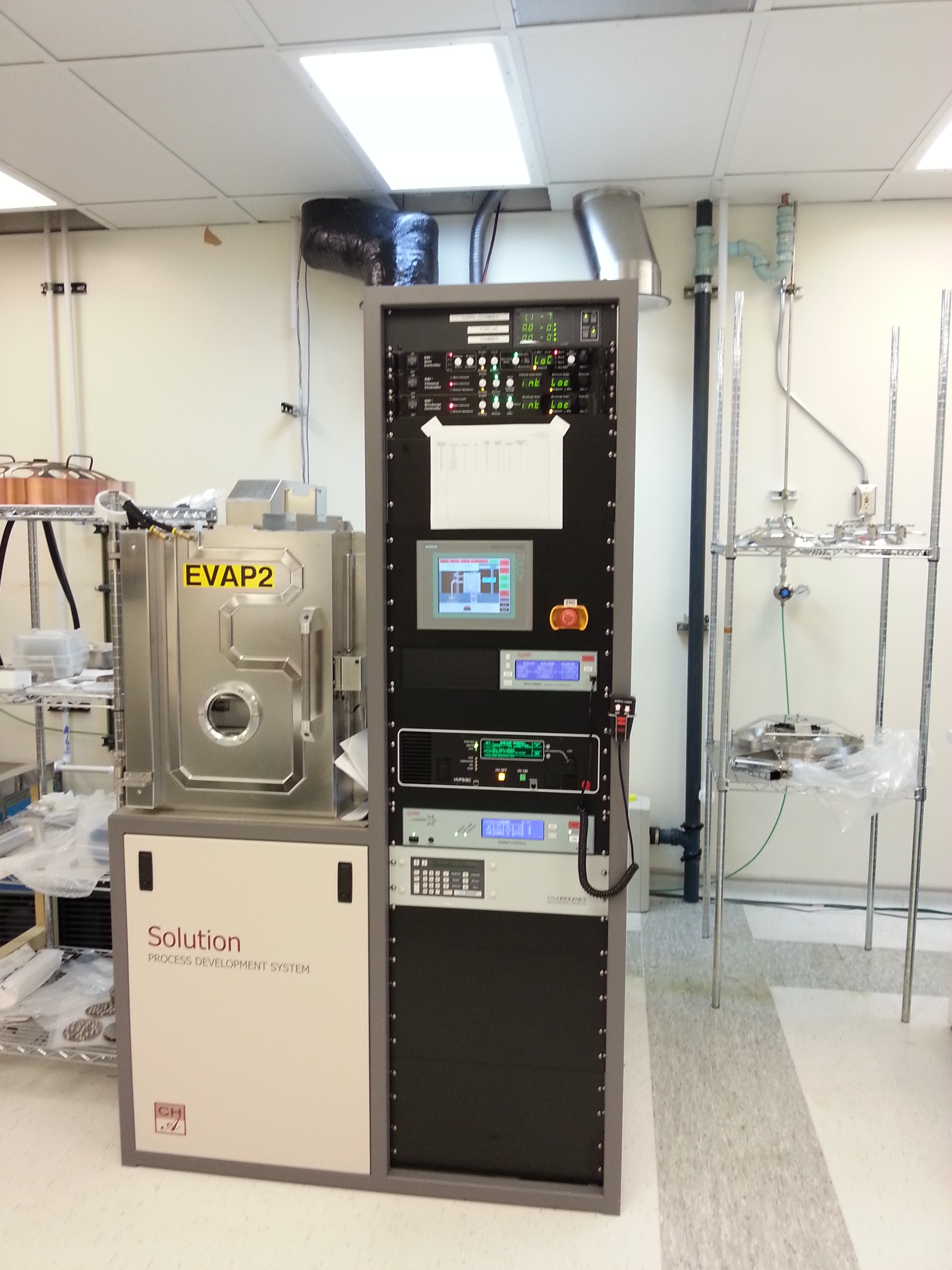
E-beam Evaporator 2
| Coral ID: | WNF--EVAP2 |
| Manufacturer: | CHA |
| Model: | Solution |
| Lab: | WNF |
| Area: | Thin Film Processing |
| Manual: | https://www.coral.washington.edu/upload/manuals/EVAP2 - SOP - 221004.pdf |
| UW Academic Rate: | $77/hr |
| Industrial Rate: | $231/hr |
| Outside Academic Rate: | $77/hr |
Description
The E-beam Evaporator is a metal evaporation system that uses an electron beam to heat the metal sources. The system has 6 pockets for different materials during deposition.
Pocket #1 is titanium, pocket #2 is chrome, Pocket #3 is gold, pocket #4 is platinum, pocked #5 is palladium or copper, and pocket #6 is aluminum.
The materials are put into crucible liners for better heat uniformity throughout the source material and to allow for easy removal and refilling. The vacuum system is produced via a cryopump as the high vacuum pump. There is a mechanical pump that is capable of roughing the chamber and regenerating the cryopump as needed.
Details
This system has a capacity of up to seven 100mm wafers when using the liftoff fixturing and fifteen 100mm wafers when using the planetary. It can also hold 3 200mm wafers in a planetary configuration. Holders for smaller pieces are also available. This system is the most automated of our evaporation systems and is capable of producing multilayer stacks without user intervention. Precious metals (Au, Pd, and Pt) are charged by use. This system also includes a heater so that depositions can be performed at up to 300 C and an ion mill to clean surfaces prior to deposition. The distance from the evaporation source to the wafer holder is about 14.5 inches.
System #6629 Solution
Gold, palladium, and platinum must be weighed before and after use. A scale for this is available next to the checkout sheet.
Make sure the gold crucible is placed on two carbon disks. The platinum crucible must make very good thermal contact with the hearth to avoid melting. Make sure the crucible fits all the way into the hearth with the top of the crucible flush with the hearth, and that the hearth is very clean before it is loaded.
Materials Restrictions
Most substrates are allowed. Consult a staff member prior to new processes on substrates other than glass, quartz, or silicon. Only pure metals are recommended. The evaporation process typically does not allow for effective deposition of compound materials. Photoresist is typically allowed, but ask a staff member prior to performing a new process.
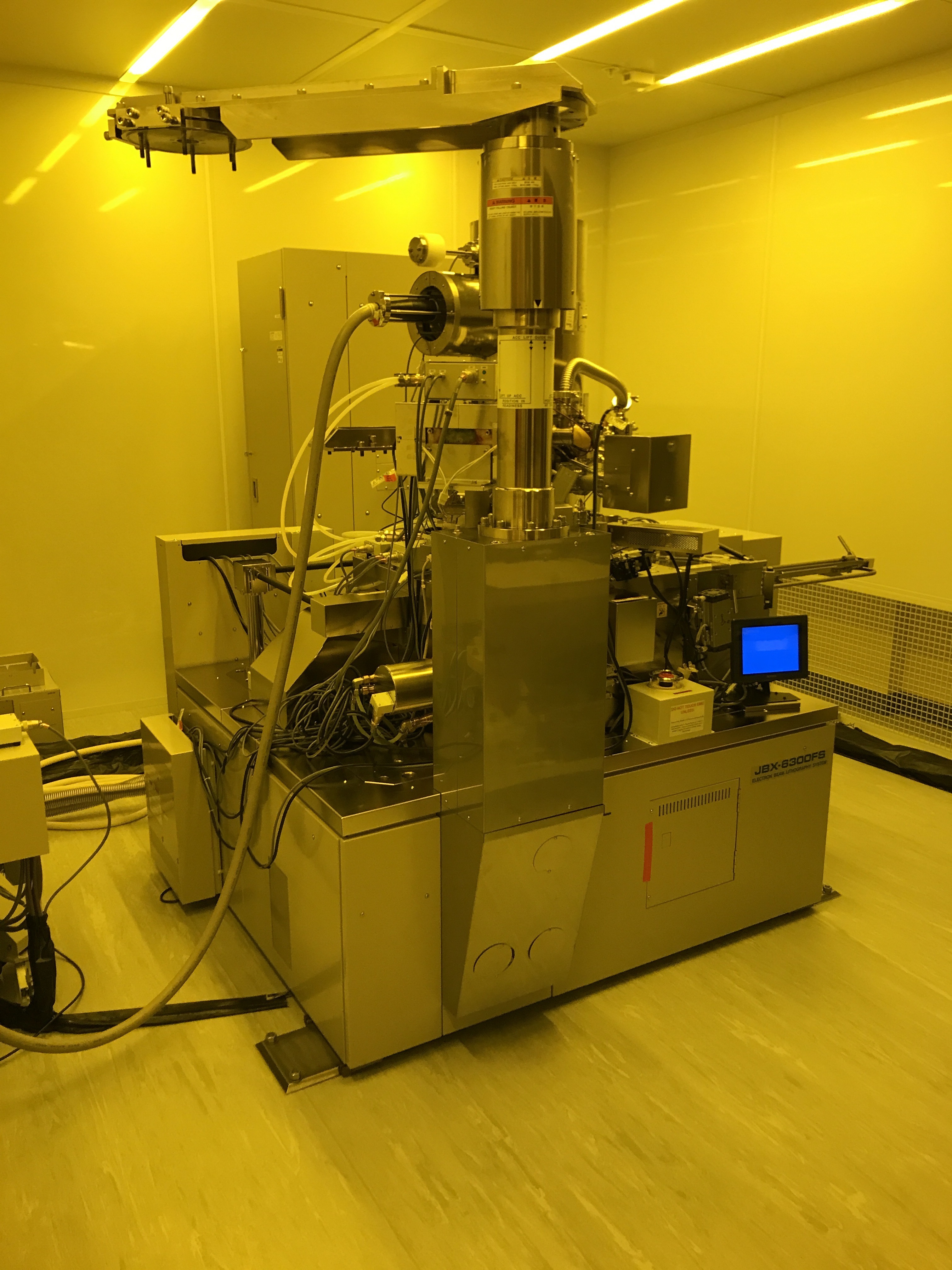
E-Beam Lithography
| Coral ID: | WNF--EBL--JEOL-JBX6300FS |
| Manufacturer: | JEOL |
| Model: | JBX6300FS |
| Lab: | WNF |
| Area: | Lithography and Direct Patterning |
| UW Academic Rate: | $137/hr |
| Industrial Rate: | $495/hr |
| Outside Academic Rate: | $137/hr |
Description
Direct-write 100 kV Electron Beam Lithography capable of feature sizes as small as 10 nm, and layer-to-layer registration better than ~30 nm m+3s.
Details
Substrates from small chips to 150mm wafers. A wide range of beam currents, choice of two objective lenses, and a wide range of resist processes provide significant flexibility for a variety of needs. Sophisticated data preparation software provides advanced functions including full shape and dose proximity correction.
Materials Restrictions
All materials must be explicitly approved by staff.
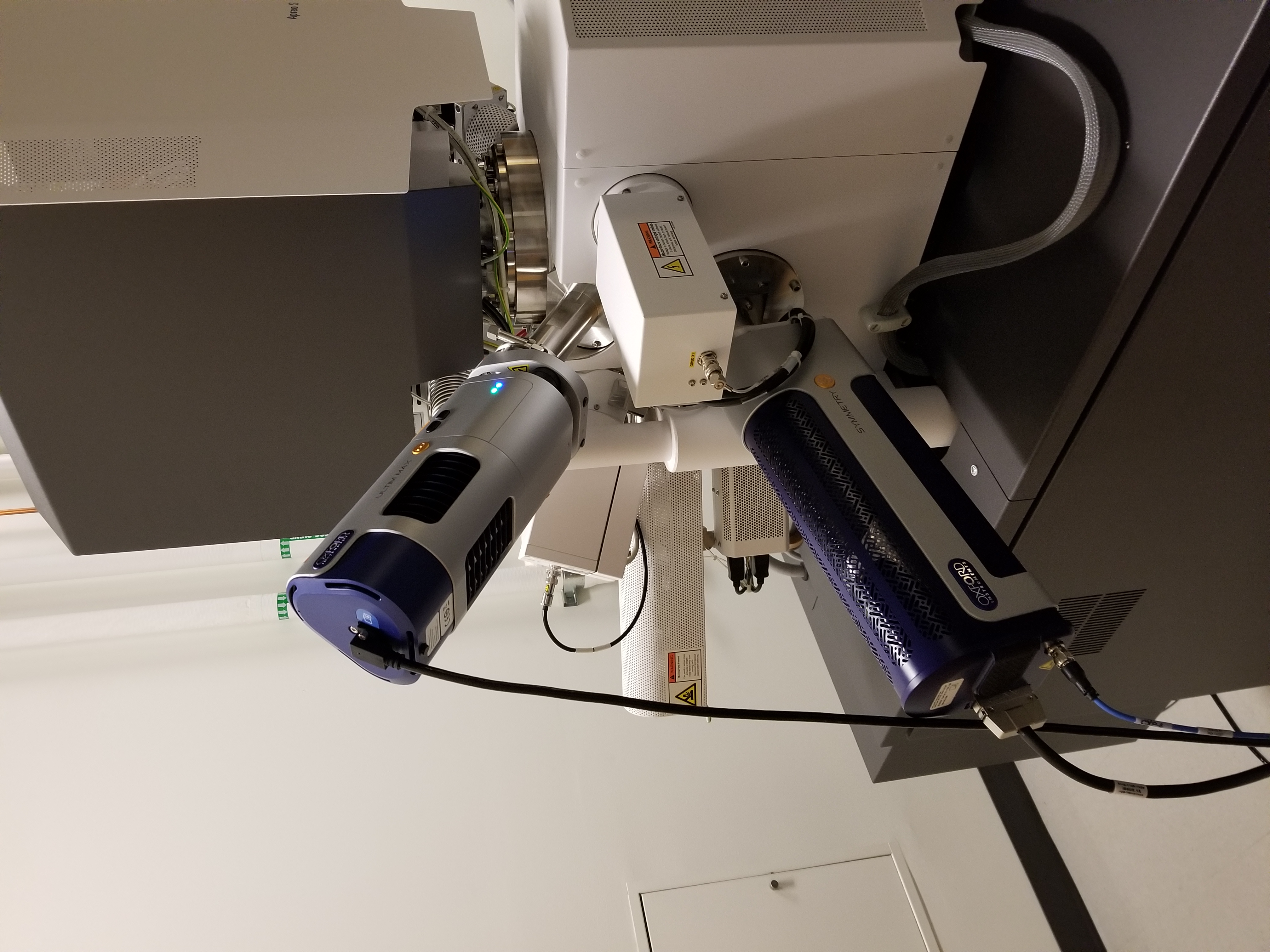
Electron Back-Scatter Diffraction (EBSD) - Apreo SEM
| Coral ID: | MAF--EBSD--Oxford-Symmetry |
| Manufacturer: | Oxford Instruments |
| Model: | Symmetry w/Ultimax 100 |
| Lab: | MAF |
| Area: | Inspection |
| UW Academic Rate: | $16/hr |
| Industrial Rate: | $50/hr |
| Internal Rate: | $0/hr |
| Non-Profit Rate: | $0/hr |
| Outside Academic Rate: | $18/hr |
Description
Oxford Insruments Symmetry Electron Back-Scatter Diffraction (EBSD) with Energy Dispersive Spectroscopy (EDS) allows grain analysis of samples in the Apreo SEM sample chamber.
Details
EBSD pixel resolution up to 1244x1024 and 4000+ fps indexed. Used for crystal orientation mapping, sample texture analysis, characterization of grain boundaries, elemental analysis, and phase discrimination. Equipped with automated Large Area Mapping, Transmission Kikuchi Diffraction (TKD) and capable of capturing EBSPs with Megapixel resolution.
Materials Restrictions
EBSD-quality polish and vacuum compatible to 10-5 Pa
Energy Dispersive X-ray Spectroscopy (EDS) - Dualbeam FIB-SEM
| Coral ID: | MAF--EDS--Dual-Beam |
| Manufacturer: | Oxford Instruments |
| Model: | X-max |
| Lab: | MAF |
| Area: | Inspection |
| Manual: | https://www.coral.washington.edu/upload/manuals/Altura EDS SOP.pdf |
| UW Academic Rate: | $6/hr |
| Industrial Rate: | $17/hr |
| Outside Academic Rate: | $7/hr |
Description
The Oxford Instruments Energy Dispersive X-ray Spectrometer (EDS) system allows elemental microanalysis of samples in the dual beam sample chamber.
Details
Demonstrated better than 125eV resolution at Mn-Ka. Aztec 3.2 with TrueLine, TrueMap, QuantLine, and automatic element deconvolution. Post-processing features are additionally available on the G44 analysis computer.
Materials Restrictions
(none)
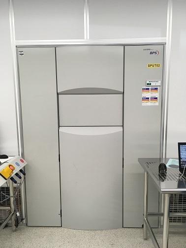
Evatec LLS EVO Sputter System
| Coral ID: | WNF--SPUT02 |
| Manufacturer: | Evatec |
| Model: | LLS EVO |
| Lab: | WNF |
| Area: | Thin Film Processing |
| Manual: | https://www.coral.washington.edu/upload/manuals/SPUT01 SPUT02 SOP.pdf |
| UW Academic Rate: | $77/hr |
| Industrial Rate: | $231/hr |
| Outside Academic Rate: | $77/hr |
Description
This turbo pumped system with a cryo pumped load lock is used for batch sputter deposition of films.
It can be used to sputter ITO, WTi, Cr, Au, and ZnO.
Details
Up to ten wafers can be loaded into the system and deposited at the same time. Wafers are loaded vertically on panels and the system sputters horizontally. The system is plumbed with nitrogen and oxygen for reactive sputtering. The system can be setup for co-sputtering. The tool has a heater and an RF sputter etcher in the load lock.
Materials Restrictions
(none)
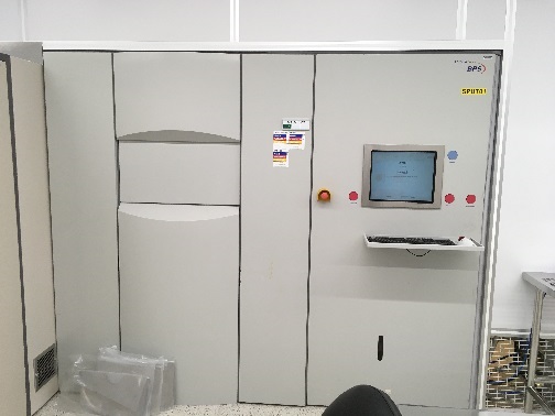
Evatec LLS EVO Sputter System
| Coral ID: | WNF--SPUT01 |
| Manufacturer: | Evatec |
| Model: | LLS EVO |
| Lab: | WNF |
| Area: | Thin Film Processing |
| Manual: | https://www.coral.washington.edu/upload/manuals/SPUT01 SPUT02 SOP.pdf |
| UW Academic Rate: | $77/hr |
| Industrial Rate: | $231/hr |
| Outside Academic Rate: | $77/hr |
Description
This turbo pumped system with a cryo pumped load lock is used for batch sputter deposition of films. It can be used to sputter Ta, Pt, Cu, Al, and Ti.
Details
Twelve wafers up to 6" diameter can be loaded into the system and deposited at the same time. Wafers are loaded vertically on panels and the system sputters horizontally. The system is plumbed with nitrogen and oxygen for reactive sputtering. The system can be setup for co-sputtering. The tool has a heater and an RF sputter etcher in the load lock.
Materials Restrictions
(none)
EVG Aligner
| Coral ID: | WNF--Aligner--EVG |
| Manufacturer: | EVG |
| Model: | 620 |
| Lab: | WNF |
| Area: | Lithography and Direct Patterning |
| Manual: | https://www.coral.washington.edu/upload/manuals/EVG-Aligner_SOPv1.1.pdf |
| UW Academic Rate: | $55/hr |
| Industrial Rate: | $165/hr |
| Outside Academic Rate: | $55/hr |
Description
Contact photolithography tool for exposure of 100mm wafers. An optimized process can achieve 2 um line/space patterns with a layer-to-layer registration accuracy about 3 um. Backside alignment is possible using a second set of alignment optics.
Details
Uses 5in square photomasks with 0.090in thickness. Configured for exposure of 100mm wafers; smaller chips can be accomodated using a carrier wafer.
Materials Restrictions
(none)
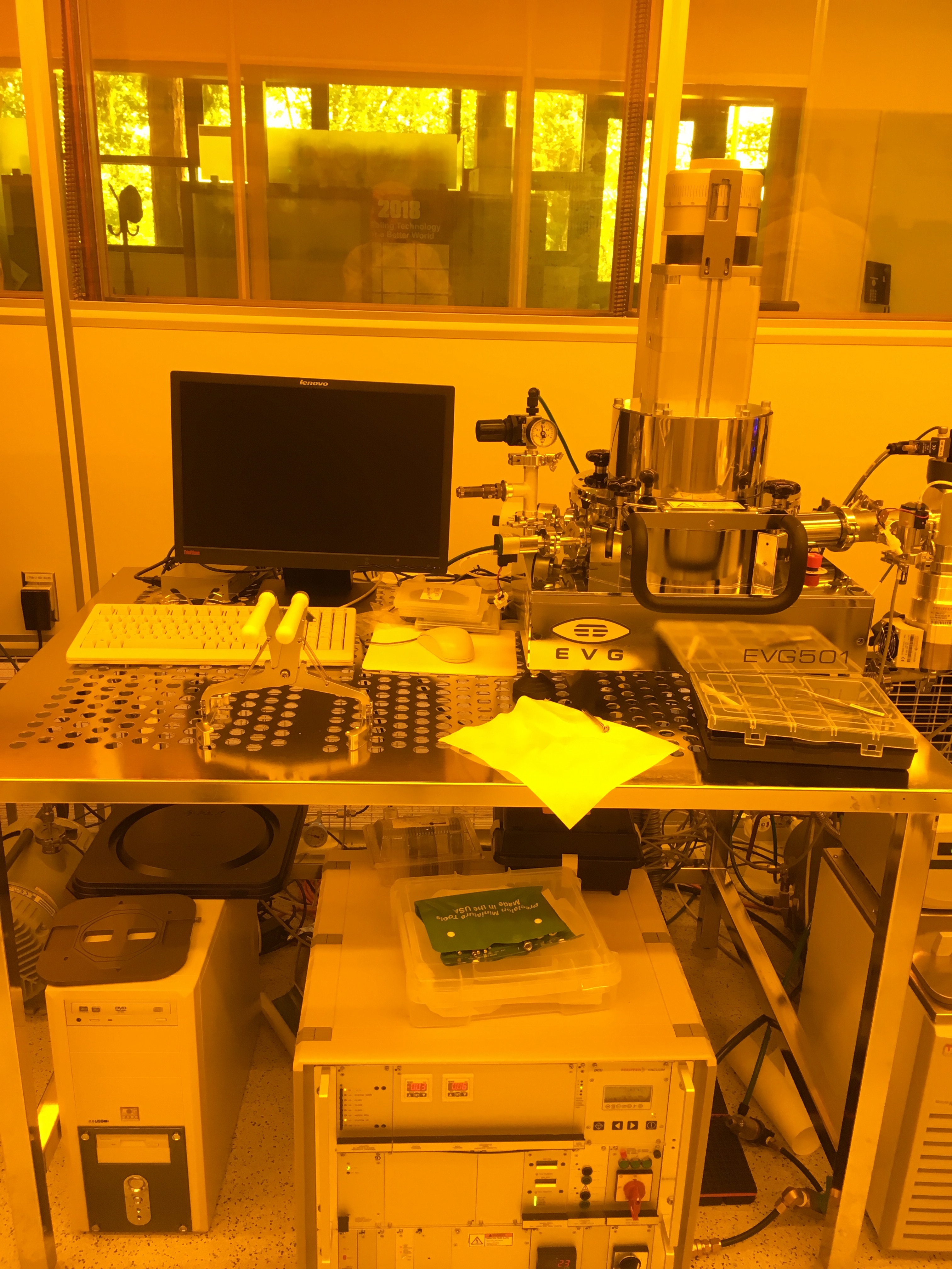
EVG Bonder
| Coral ID: | WNF--Bonder--EVG |
| Manufacturer: | EVG |
| Model: | 501 |
| Lab: | WNF |
| Area: | Packaging and Back End |
| Manual: | https://www.coral.washington.edu/upload/manuals/EVGBond_SOPv1.4.pdf |
| UW Academic Rate: | $77/hr |
| Industrial Rate: | $231/hr |
| Outside Academic Rate: | $77/hr |
Description
Thermal compression anodic bonding for Si and glass substrates.
Details
Configured for 100mm wafers.
Materials Restrictions
(none)
Expertech CTR200 Anneal Furnace
| Coral ID: | WNF--Furnace--Anneal |
| Manufacturer: | Expertech |
| Model: | CTR200 |
| Lab: | WNF |
| Area: | Thin Film Processing |
| Manual: | https://www.coral.washington.edu/upload/manuals/Atmospheric Furnace SOP 20180828.pdf |
| UW Academic Rate: | $11/hr |
| Industrial Rate: | $33/hr |
| Outside Academic Rate: | $11/hr |
Description
This atmospheric tube furnace is capable of both dry oxidation and annealing.
Details
This anneal furnace has a maximum temperature of 1000C. It is plumbed with nitrogen, oxygen, and forming gas (2% H2 in N2). It can accommodate 44 wafers with diameters up to 200 mm. Irregular samples can be arranged with staff.
Materials Restrictions
This furnace does allow wafers contaminated with metals. Materials must be robust at the maximum temperature called for in the recipe.
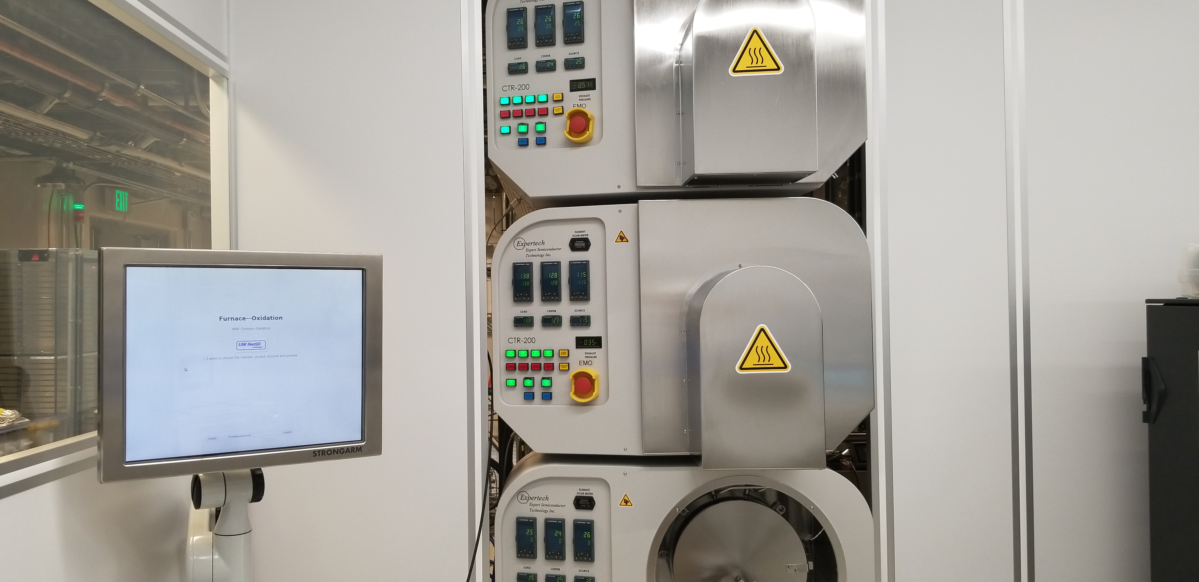
Expertech CTR200 Oxidation Furnace
| Coral ID: | WNF--Furnace--Oxidation |
| Manufacturer: | Expertech |
| Model: | CTR200 |
| Lab: | WNF |
| Area: | Thin Film Processing |
| Manual: | https://www.coral.washington.edu/upload/manuals/Atmospheric Furnace SOP 20180828.pdf |
| UW Academic Rate: | $11/hr |
| Industrial Rate: | $33/hr |
| Outside Academic Rate: | $11/hr |
Description
This atmospheric tube furnace is capable of both wet and dry oxidation.
Details
It has a maximum temperature of 1000C. It is plumbed with nitrogen, oxygen, and steam from a deionized water bubbler. It can accommodate 44 wafers with diameters up to 200 mm. Irregular samples can be arranged with staff.
Materials Restrictions
This furnace does not allow any metal-contaminated wafers. Wafers must be clean before oxidation.
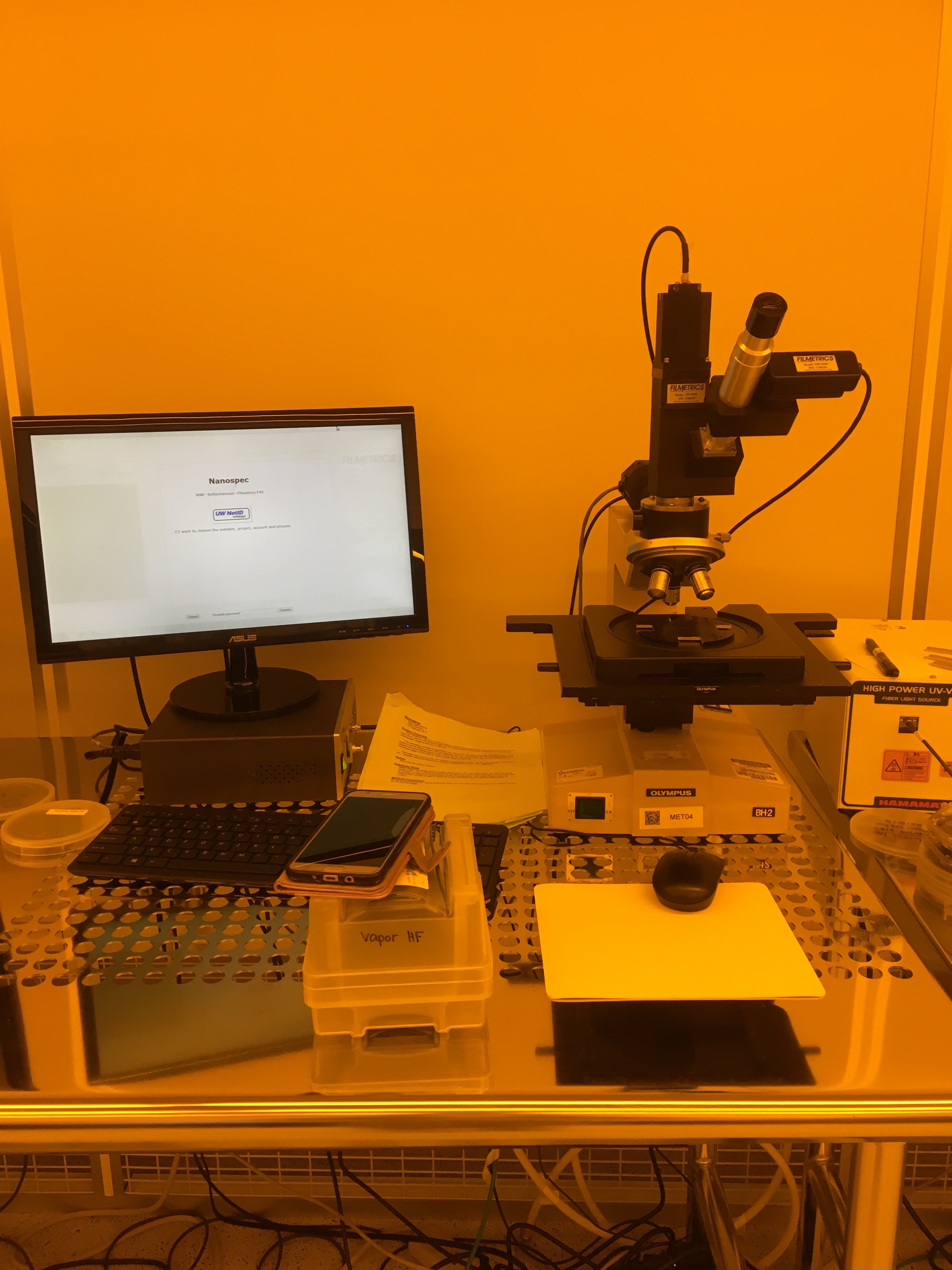
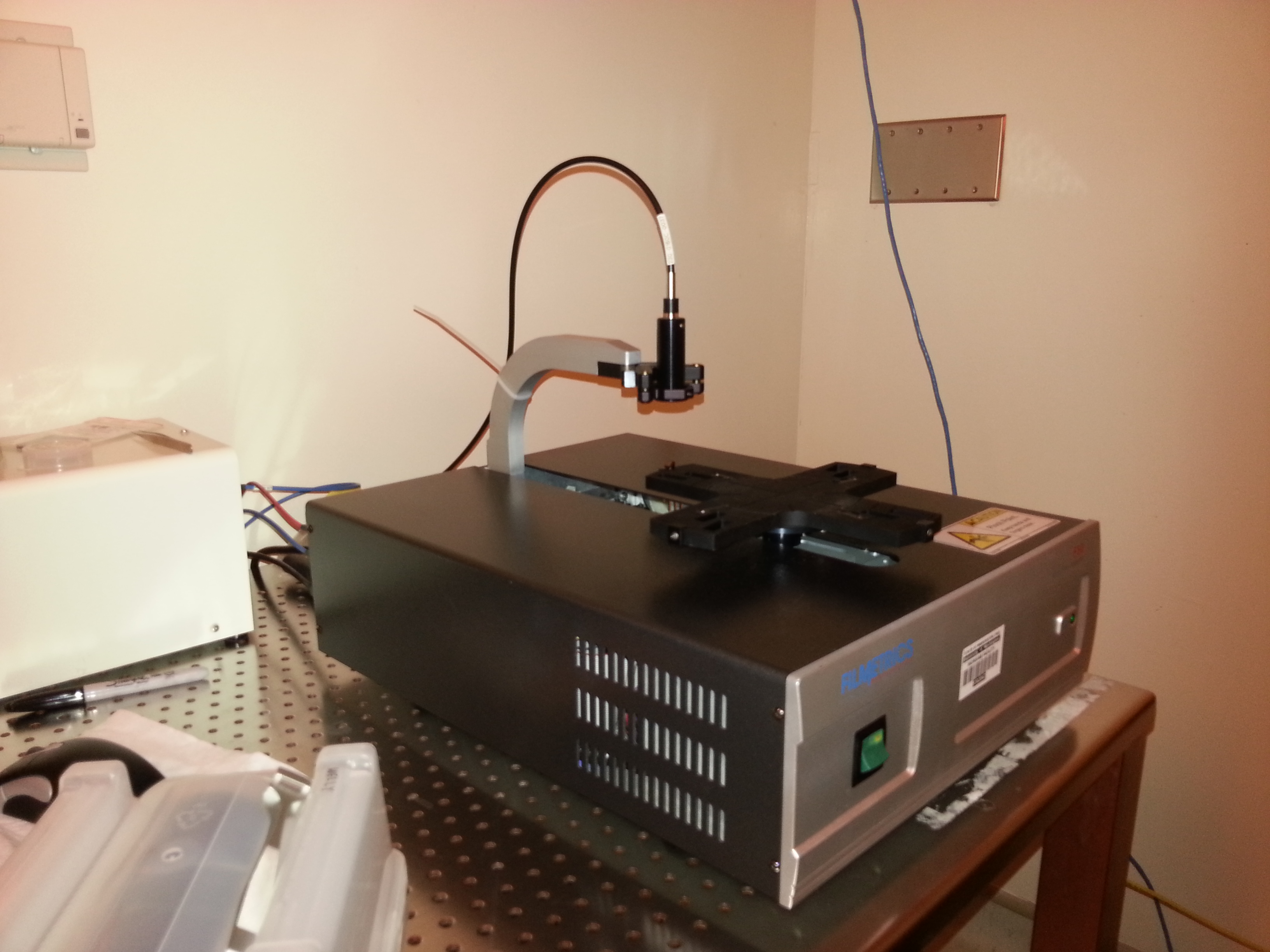
Filmetrics F40 Small Point Reflectometer
| Coral ID: | WNF--Reflectometer--Filmetrics-F40 |
| Manufacturer: | Filmetrics |
| Model: | 210 |
| Lab: | WNF |
| Area: | Thin Film and Materials Characterization |
| Manual: | https://www.coral.washington.edu/upload/manuals/Nanospec SOP 20170216.pdf |
| UW Academic Rate: | $11/hr |
| Industrial Rate: | $33/hr |
| Outside Academic Rate: | $11/hr |
Description
Single-point spectral reflectance to measure film thickness and refractive index.
Details
(none given)
Materials Restrictions
(none)
Filmetrics F50 Thin Film Reflectometer
| Coral ID: | WNF--Reflectometer--Filmetrics-F50 |
| Manufacturer: | Filmetrics |
| Model: | F50 |
| Lab: | WNF |
| Area: | Device and Structure Characterization |
| Manual: | https://www.coral.washington.edu/upload/manuals/FilmetricsUserInstructions_V1.0.pdf |
| UW Academic Rate: | $11/hr |
| Industrial Rate: | $33/hr |
| Outside Academic Rate: | $11/hr |
Description
Optical measurement of thin film layers on various substrates. Uses spectral reflectance to determine film thickness, refractive index, and extinction coefficient by scanning wavelengths from 200 to 1700 nm. Substrates up to 150 mm can be mapped automatically.
Details
(none given)
Materials Restrictions
(none)
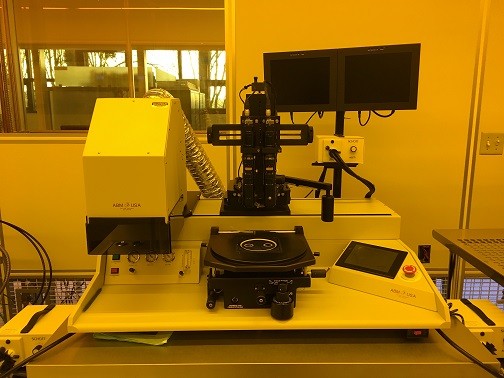
Finetech Fineplacer pico
| Coral ID: | WNF--WireBonder--Flip-Chip |
| Manufacturer: | Finetech |
| Model: | Fineplacer pico |
| Lab: | WNF |
| Area: | Packaging and Back End |
| Manual: | https://www.coral.washington.edu/upload/manuals/flipchip_SOP_2.1.pdf |
| UW Academic Rate: | $55/hr |
| Industrial Rate: | $165/hr |
| Outside Academic Rate: | $55/hr |
Description
This flip chip and die bonder can be used to place parts with better than 5um accuracy.
Details
(none given)
Materials Restrictions
(none)
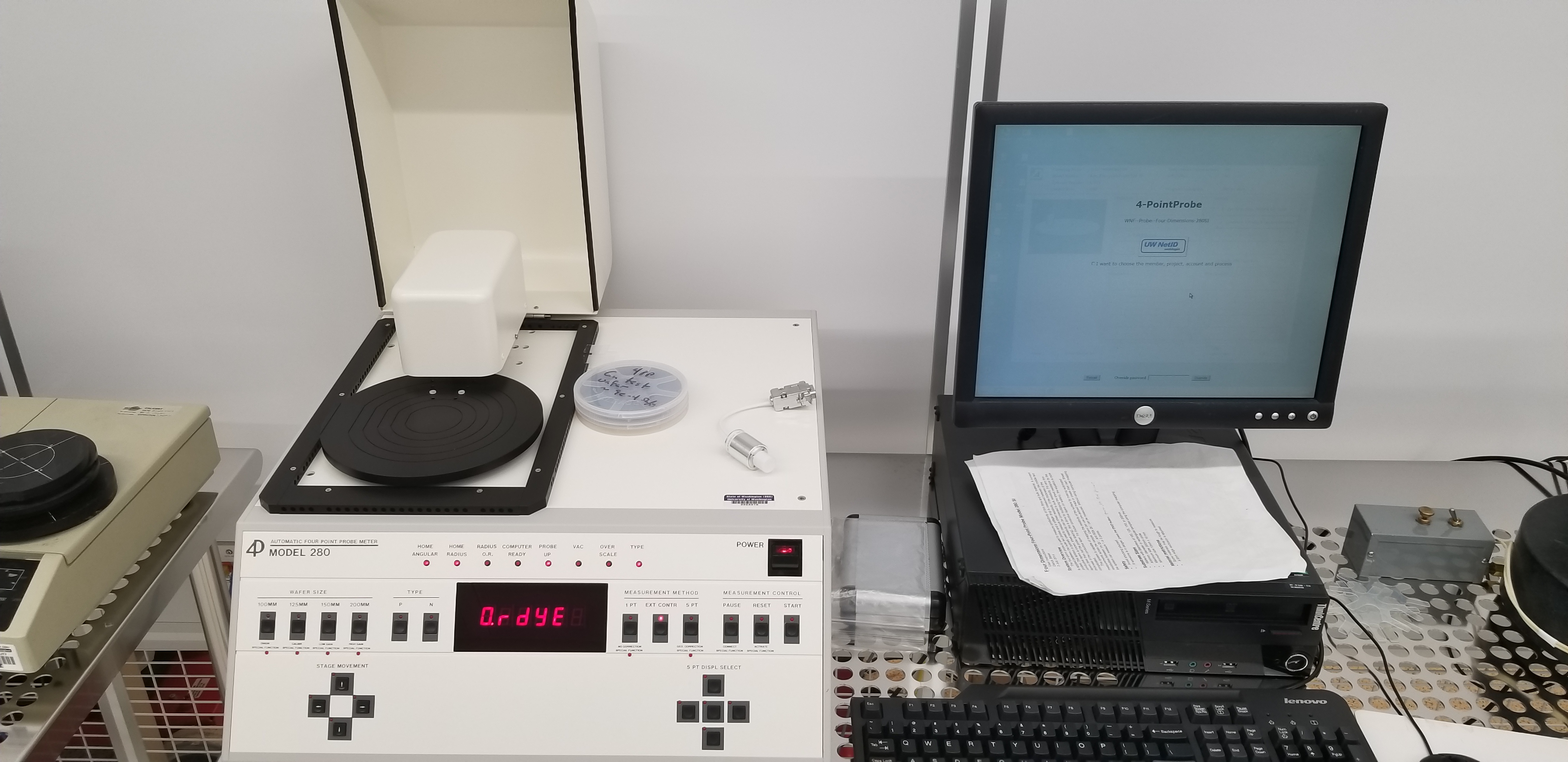
Four Dimensions Four-Point Probe Model 280 SI
| Coral ID: | WNF--Probe--Four-Dimensions-280SI |
| Manufacturer: | Four Dimensions |
| Model: | 280 SI |
| Lab: | WNF |
| Area: | Thin Film and Materials Characterization |
| Manual: | https://www.coral.washington.edu/upload/manuals/Four-Point Probe SOP.pdf |
| UW Academic Rate: | $0/hr |
| Industrial Rate: | $0/hr |
| Outside Academic Rate: | $0/hr |
Description
The Four Dimensions Four-Point Probe Model 280 SI is capable for making sheet resistivity measurements on various samples. It can map the sheet resistance of samples up to 8 inches in diameter. There are standard maps in the system and custom maps can be created.
Details
The four-point probe is used to measure conductivity of thin films and bulk material. A current is applied between the outer two probes and a voltage drop is measured between the middle two probes. This system is typically used to measure sheet resistivity, if the thickness of the conductive layers is known, sheet resistivity can be converted to bulk resistivity
Materials Restrictions
Make sure samples are dry and clean before loading them into the four-point probe. For samples thicker than a wafer, make sure the probe head will clear the sample.

Gatan Solarus Plasma Cleaner
| Coral ID: | MAF--Plasma-Cleaner--Gatan-Solarus |
| Manufacturer: | Gatan |
| Model: | Solarus |
| Lab: | MAF |
| UW Academic Rate: | $0/hr |
| Industrial Rate: | $0/hr |
| Outside Academic Rate: | $0/hr |
Description
Plasma clean and glow-discharge samples which are compatible with HV systems or TEM holders.
Details
Top down chamber for "large" bulky samples or TEM grids; Two side mount chambers for TEM holders.
Materials Restrictions
Staff training and qualification required for use. Samples must be approved for use in the chambers.
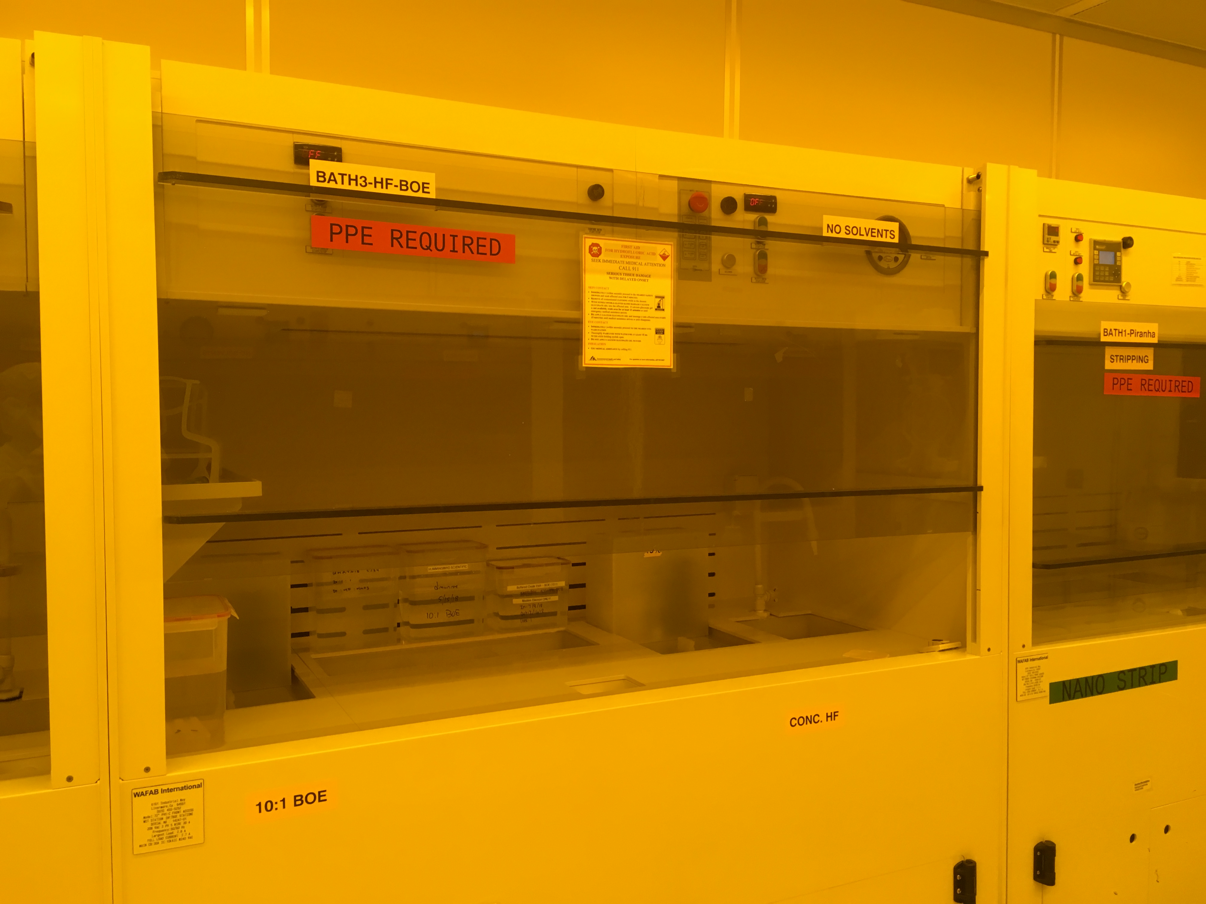
HF and BOE process station
| Coral ID: | WNF--BATH3-HF-BOE |
| Manufacturer: | WAFAB International |
| Model: | 72" PVC-C Front Access Wet Station (HF/BOE Station) |
| Lab: | WNF |
| Area: | Wet Etch and Cleaning |
| Manual: | https://www.coral.washington.edu/upload/manuals/BATH3-HF-BOE_3.0.pdf |
| UW Academic Rate: | $0/hr |
| Industrial Rate: | $0/hr |
| Outside Academic Rate: | $0/hr |
Description
Wet bench dedicated to processing with HF containing materials.
Details
Refilled by request
Materials Restrictions
(none)

HMDS/Image Reversal Oven
| Coral ID: | WNF--YES-Oven |
| Manufacturer: | Yield Engineering Systems |
| Model: | YES-58 |
| Lab: | WNF |
| Manual: | https://www.coral.washington.edu/upload/manuals/YES58-Oven_SOP_20240411.pdf |
| UW Academic Rate: | $33/hr |
| Industrial Rate: | $99/hr |
| Outside Academic Rate: | $33/hr |
Description
HMDS oven for priming wafers. Has image reversal capability, but ammonia is currently not hooked up to the system.
Details
(none given)
Materials Restrictions
(none)
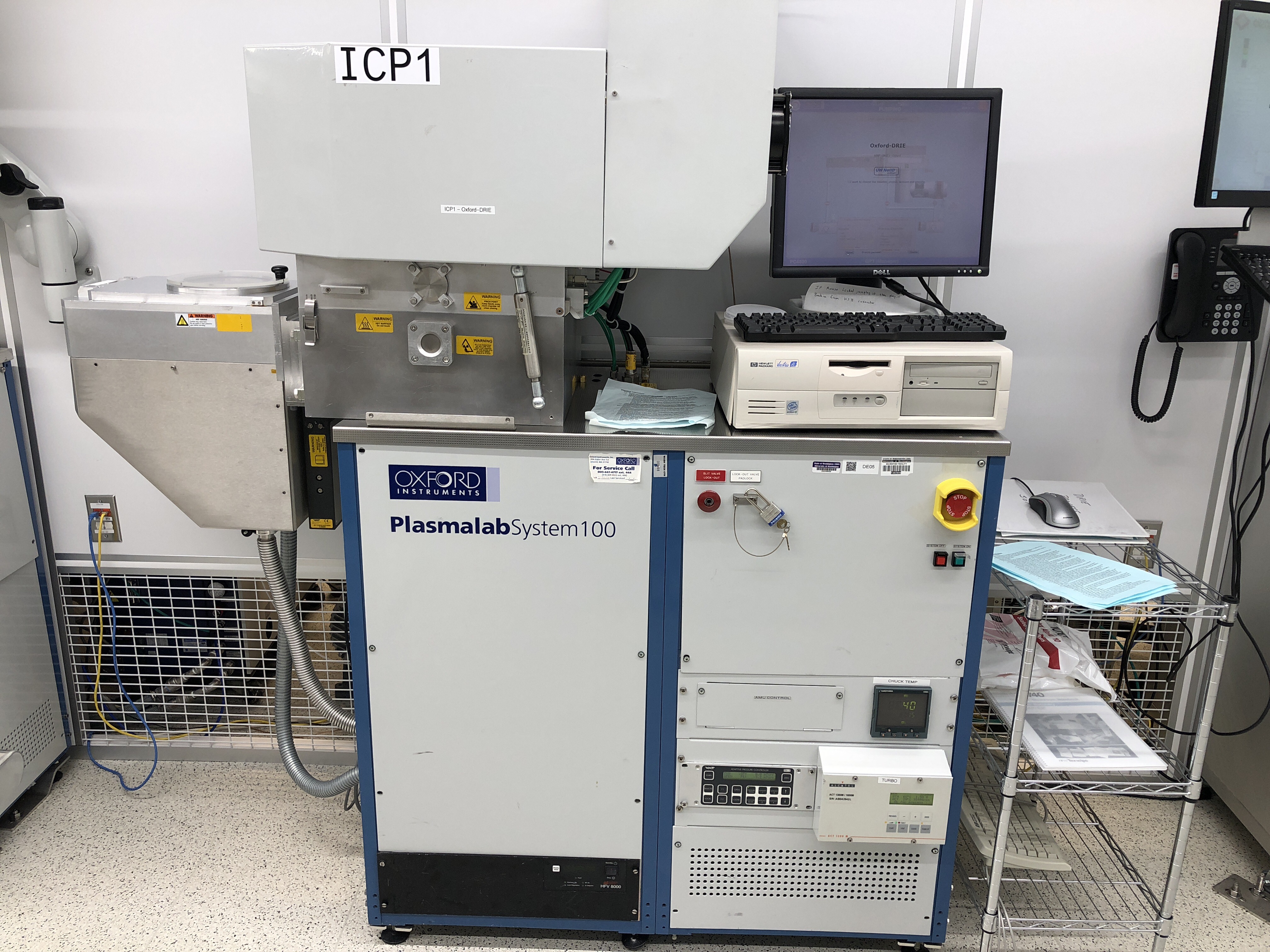
ICP Plasma Etcher
| Coral ID: | WNF--DRIE1--Oxford |
| Manufacturer: | Oxford Instruments |
| Model: | ICP 380 |
| Lab: | WNF |
| Area: | Dry Etch |
| Manual: | https://www.coral.washington.edu/upload/manuals/ICP1-SpecialMaterial-Oxford_SOPv5.pdf |
| UW Academic Rate: | $77/hr |
| Industrial Rate: | $231/hr |
| Outside Academic Rate: | $77/hr |
Description
ICP Etch system for etching Lithium Niobate, 2-D materials (WSe2, BN, MoS2...) and other special materials.
Details
100mm wafers - chips must use a 100mm carrier wafer with die attach via Fomblin or Stantovac vacuum oils. Available process gases: SF6 (0-100sccm), O2 (0-100sccm), C4F8 (0-100sccm), Ar (0-100sccm). NOTE: Tool configuration alternates between Lithium-Niobate-only-etching and Non-Lithium-Niobate-etching. Each configuration has a dedicated quartz clamp ring with extensive manual and plasma chamber cleaning occurring during the re-configuration. Generally, the configuration schedule alternates on a weekly basis; however, this regime may deviate from this depending on user requirements. Please see tool owner for details. Current configuration can be found in Coral comments for this tool (search both 'unresolved' and 'resolved' comments).
Materials Restrictions
100mm wafers or dies/chips attached to 100mm carrier wafer. Allowed etch target materials: Silicon, Silicon Oxide, Silicon Nitride, Lithium Niobate, 2D materials, PMDS, Polyimide, Parylene, Graphene, Niobium, Lithium Niobate, some refractory metals. Allowed mask materials: Photoresist, E-Beam Resist, SiO2, Silicon Nitride, Alumina, some metal masks. Please see tool owner to discuss and gain permission for other hard mask materials, including metal masks. No exposed Copper, Gold, nor Silver. No high-vapor-pressure materials. Please contact the tool owner to discuss materials not included on this list.
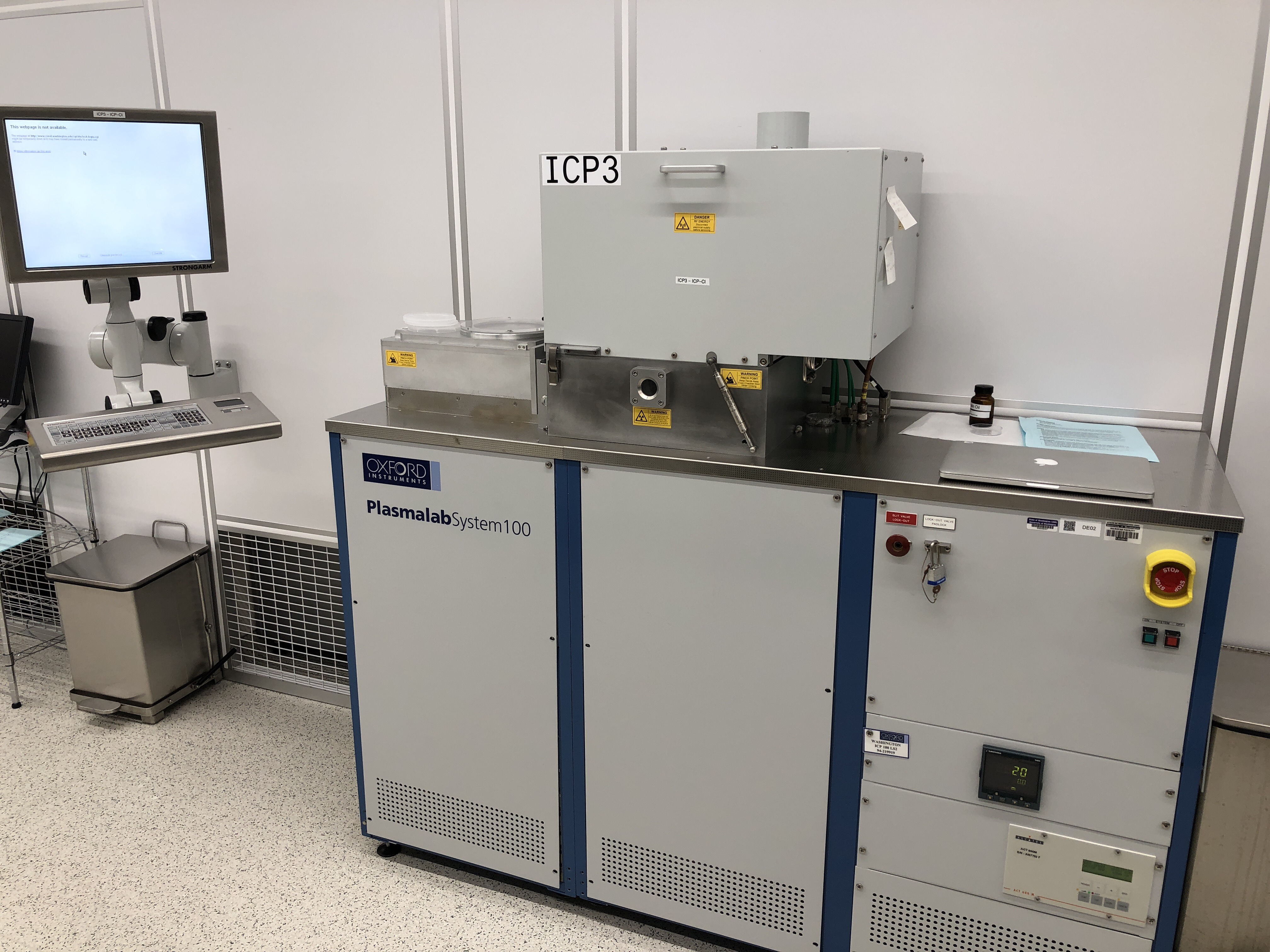
ICP-Chlorine
| Coral ID: | WNF--ICP--Oxford-Chlorine |
| Manufacturer: | Oxford |
| Model: | PlasmaLab 100, ICP-180 |
| Lab: | WNF |
| Area: | Dry Etch |
| Manual: | https://www.coral.washington.edu/upload/manuals/ICP3-Cl-Oxford_UserManual_v5.1.pdf |
| UW Academic Rate: | $77/hr |
| Industrial Rate: | $231/hr |
| Outside Academic Rate: | $77/hr |
Description
Highly anisotropic Inductively Coupled Plasma (ICP) etching using chlorine-based etch chemistries for etching Silicon, III-V semiconductors, aluminum and chrome. Load-locked for rapid load/unload and high process consistency. See tool owner for specific material restrictions.
Details
Process gases: BCl3, Cl2, H2, N2, O2, CH4, SF6, and Ar. A heated stage allows etching at substrates temperatures up to 250 C. 100mm wafers only. Smaller sizes can be accomodated using a 100mm silicon wafer as a carrier wafer (Users must supply their own carrier wafer - do not use the system dummy wafer as a carrier). Please take note of new policy changes outlined under 'Restrictions' in the ICP-C's SOP concerning resist edge-bead removal and oxygen process gas.
Materials Restrictions
Allowed etch target materials: Silicon, Silicon Dioxide (see below), Silicon Nitride, GaAs, GaP, GaN, AlN, InP, Al, Cr, Ti. Contact tool owner for other III-V and II-VI materials. Allowed mask materials: Photoresist, E-Beam Resist, SiO2, Silicon Nitride, Alumina. Metal masks not allowed. No exposed noble metals including copper. Do not etch quartz nor fused silica. Note: Certain III-V compounds require elevated chuck temperatures - see tool owner. No high-vapor-pressure materials. Please contact tool owner to discuss materials not included on this list.
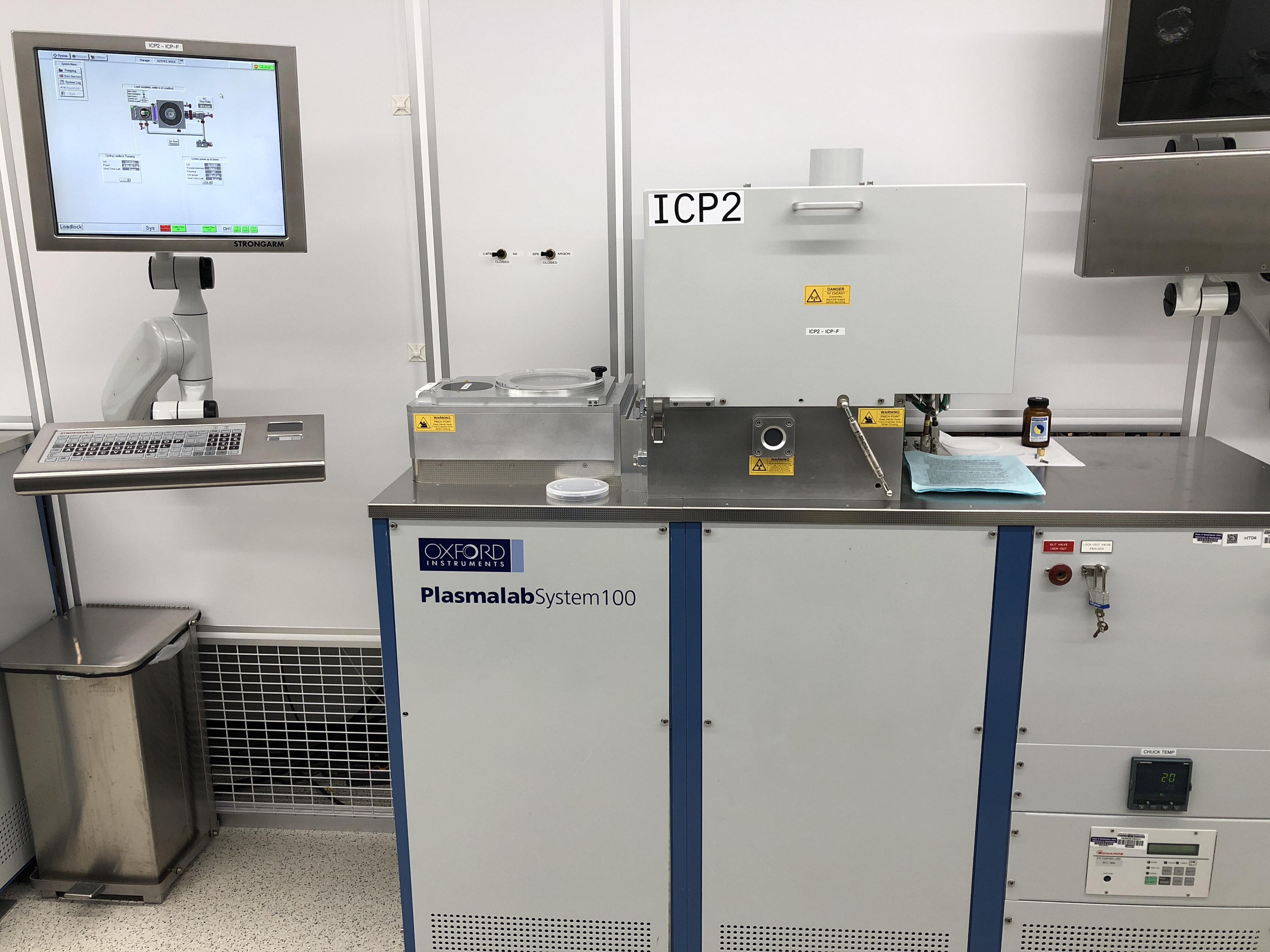
ICP-Fluorine
| Coral ID: | WNF--ICP--Oxford-Fluorine |
| Manufacturer: | Oxford |
| Model: | PlasmaLab 100, ICP-180 |
| Lab: | WNF |
| Area: | Dry Etch |
| Manual: | https://www.coral.washington.edu/upload/manuals/ICP2-F-Oxford_UserSOP_v79.pdf |
| UW Academic Rate: | $77/hr |
| Industrial Rate: | $231/hr |
| Outside Academic Rate: | $77/hr |
Description
Plasma tool capable of highly anisotropic etching using fluorine-based etch chemistries. Additionally, isotropic etching is available via ICP-only configuration. Load-locked for rapid load/unload and good process consistency. Wafer stage is temperature controlled via chilled nitrogen gas - upon request, additional LN2-cooling is available for cryo-etching. NOTE: New chamber cleaning policy: all chamber cleaning must be done with the system enabled and, at intervals of no more than 15 minutes, users must confirm the clean process continues to run to completion without error. The tool may be disabled only if there is less than 15 minutes left on the clean.
Details
Process gases: C4F8, CHF3, N2, O2, Ar, and SF6. 100mm wafers only. Smaller sizes can be accomodated using a 100mm silicon wafer as a carrier wafer.
Materials Restrictions
Allowed etch target materials: Silicon, Silicon Dioxide (see below), Silicon Nitride, some refractory metals including Tungsten and Molybdenum, SiC, Polyimide, Parylene, Graphene. Allowed mask materials: Photoresist, E-Beam Resist, SiO2, Silicon Nitride, Alumina. (Metal masks are not allowed.) No dirty glass can be etched (<99% SiO2), ie no pyrex, no borosilicate, no soda-lime. No exposed metal including copper, gold, and silver. Note: SiO2 (quartz and fused silica) are limited to 4um total etch depth. No high-vapor-pressure materials. Please contact tool owner to discuss materials not included on this list.
ICP-MatthewsIntl-ChlorinePZT
| Coral ID: | WNF--ICP05-Oxford |
| Manufacturer: | Oxford |
| Lab: | WNF |
| Area: | Dry Etch |
Description
This chlorine chemistry, PZT targeted, dry etch tool is owned by Matthews International. User access is limited, contact tool owner for information.
Details
(none given)
Materials Restrictions
(none)
In-situ SEM Indenter
| Coral ID: | MAF--Indentor--Alemnis |
| Manufacturer: | Alemnis |
| Model: | Standard Assembly |
| Lab: | MAF |
| Area: | Thin Film and Materials Characterization |
| Manual: | https://www.coral.washington.edu/upload/manuals/Alemnis ASA Setup - Apreo.pdf |
| UW Academic Rate: | $0/hr |
| Industrial Rate: | $0/hr |
| Outside Academic Rate: | $0/hr |
Description
The Alemnis Standard Assembly (ASA) allows mechanical testing of samples in the SEM chamber with video capture.
Details
Test hardness, modulus of elasticity, residual stress, time-dependent creep and relaxation, fracture toughness and fatigue on thinfilms without removing the substrate. Max load 500mN.
Materials Restrictions
Samples must be vacuum-compatible and no larger than 25mm diameter, 1cm tall.
Ion Mill
| Coral ID: | MAF--Ion-Mill--Fischione-1050 |
| Manufacturer: | Fischione |
| Model: | TEM Mill |
| Lab: | MAF |
| UW Academic Rate: | $34/hr |
| Industrial Rate: | $126/hr |
| Outside Academic Rate: | $40/hr |
Description
The Fischione TEM Mill is an ion polishing instrument used for the final thinning and polishing of hard (conventional) materials prior to TEM analysis.
Details
Two penning ion sources use Argon ions at 1-6kV to mill one or both sides of a 3mm diameter disc. Adjustable angle from 10 to -10 degree incidence.
Materials Restrictions
(none)
Isothermal Titration Calorimeter
| Coral ID: | MAF--ITC--AUTOITC200 |
| Manufacturer: | Microcal |
| Model: | AutoITC200 |
| Lab: | MAF |
| Area: | Biological/Chemical/Particle Technology |
| UW Academic Rate: | $22/hr |
| Industrial Rate: | $126/hr |
| Outside Academic Rate: | $26/hr |
Description
Measures heat of binding, Kd, stoichiometry, Entropy and Free energy of binding
Details
(none given)
Materials Restrictions
(none)
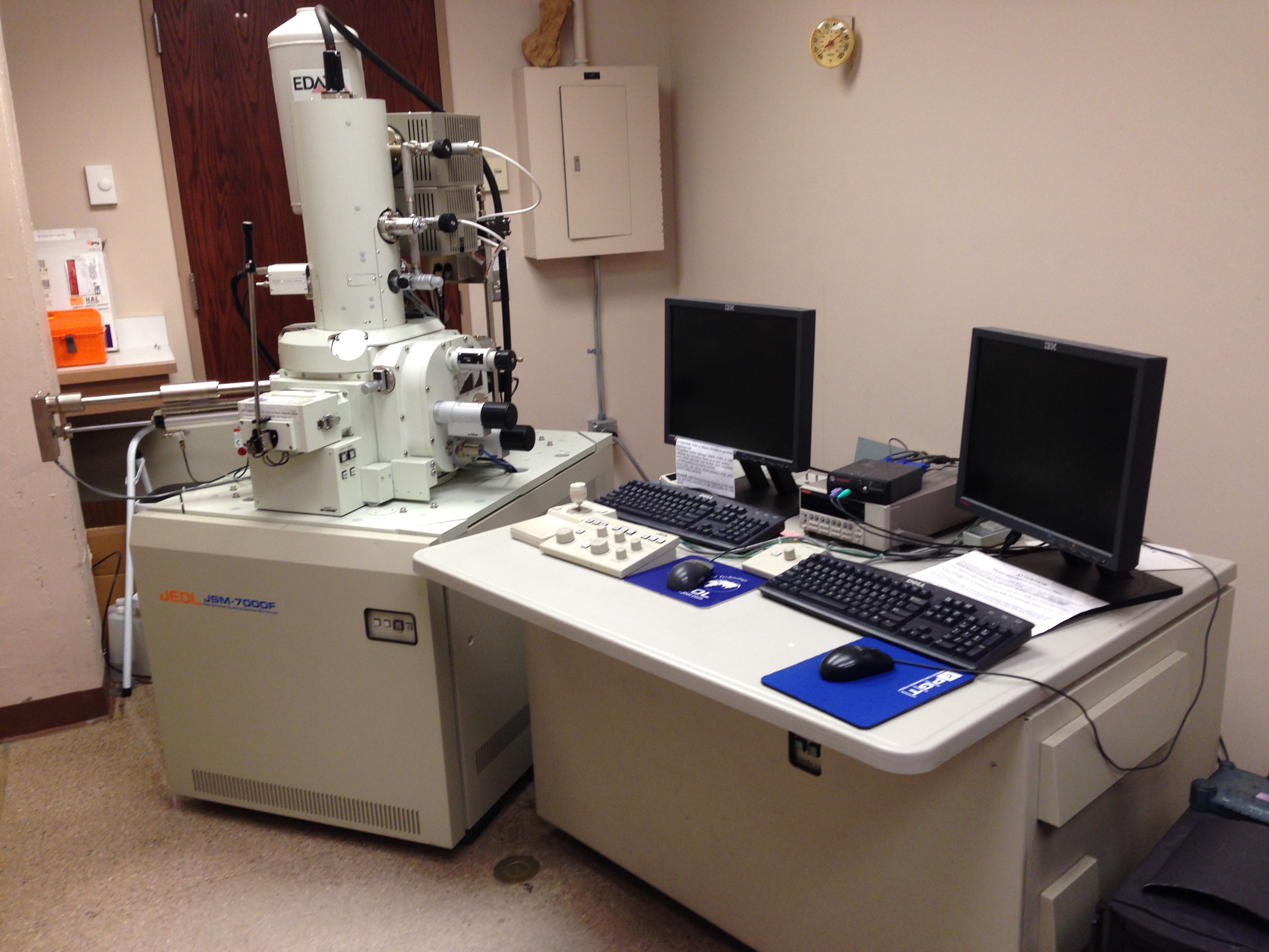
JEOL JSM 7000F Analytical SEM
| Coral ID: | MSE--SEM--JEOL-JSM7000F |
| Manufacturer: | JEOL |
| Model: | JSM 7000F |
| Lab: | MSE |
| UW Academic Rate: | $50/hr |
| Industrial Rate: | $180/hr |
| Outside Academic Rate: | $50/hr |
Description
Scanning Electron Microscope
Details
(none given)
Materials Restrictions
(none)
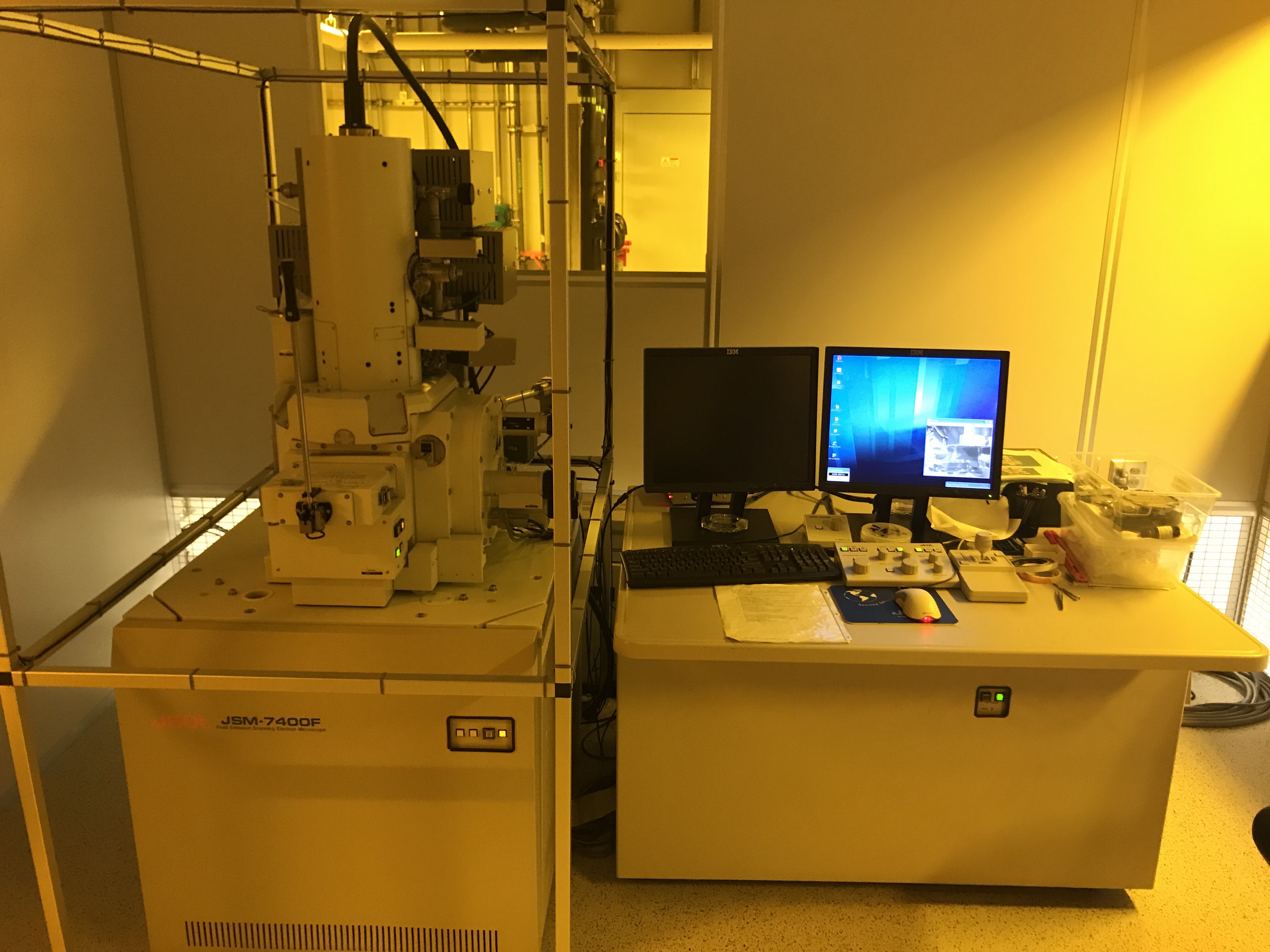
JEOL-SEM
| Coral ID: | WNF--SEM--JEOL-JSM7400F |
| Manufacturer: | JEOL |
| Model: | JSM7400F |
| Lab: | WNF |
| Area: | Device and Structure Characterization |
| Manual: | https://www.coral.washington.edu/upload/manuals/JSM7400F_SEM_user_instructions_2.0.pdf |
| UW Academic Rate: | $77/hr |
| Industrial Rate: | $231/hr |
| Outside Academic Rate: | $77/hr |
Description
Very high-resolution cold field emission Scanning Electron Microscope (SEM), provides imaging down to a few nm. Conventional, in-lens and backscattered electron detectors are available.
Details
A load-lock allows fast sample exchange and maintains a clean chamber for better high-resolution imaging. A variety of sample holders for mounting substrates from small chips up to 100mm wafers. Tilt angle range depends on substrate size and working distance.
Materials Restrictions
Clean, low-outgassing substrates only. No magnetic samples.
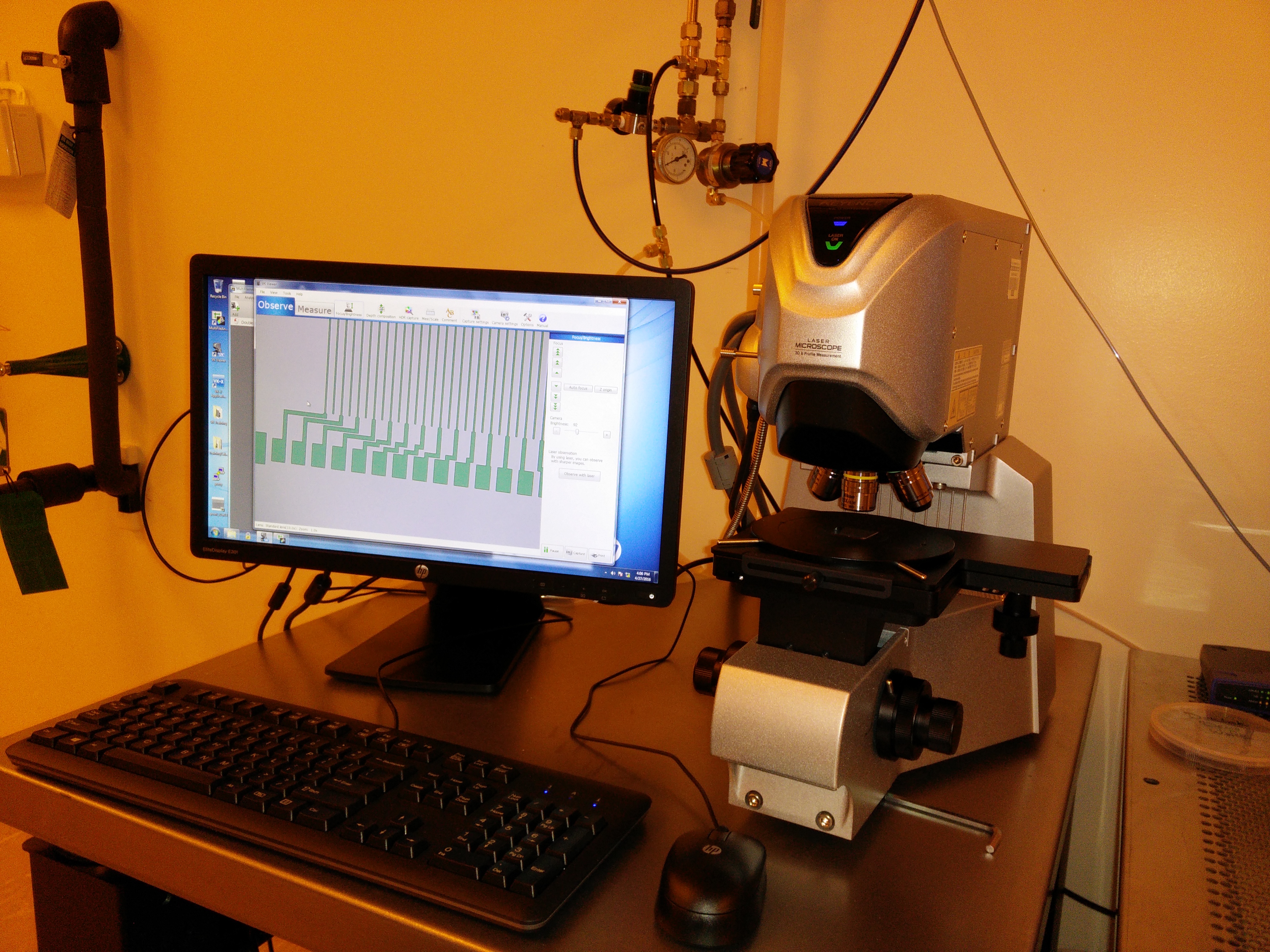
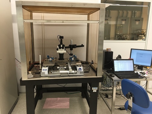
Keyence Laser Scanning Confocal Microscope
| Coral ID: | WNF--Confocal-Microscope--Keyence-VK-X150K |
| Manufacturer: | Keyence |
| Model: | VK-X150K |
| Lab: | WNF |
| Area: | Device and Structure Characterization |
| Manual: | https://www.coral.washington.edu/upload/manuals/Keyence_SOP1_1.pdf |
| UW Academic Rate: | $11/hr |
| Industrial Rate: | $33/hr |
| Outside Academic Rate: | $11/hr |
Description
This laser scanning confocal microscope obtains 3D measurements from a wafer surface for measurement of both step heights and lateral dimensions. This model uses a red (658 nm) laser. The step height measurement has a resolution of 5 nm with a minimum step height of 50 nm. Lateral measurements have a resolution of 250 nm.
Details
(none given)
Materials Restrictions
(none)
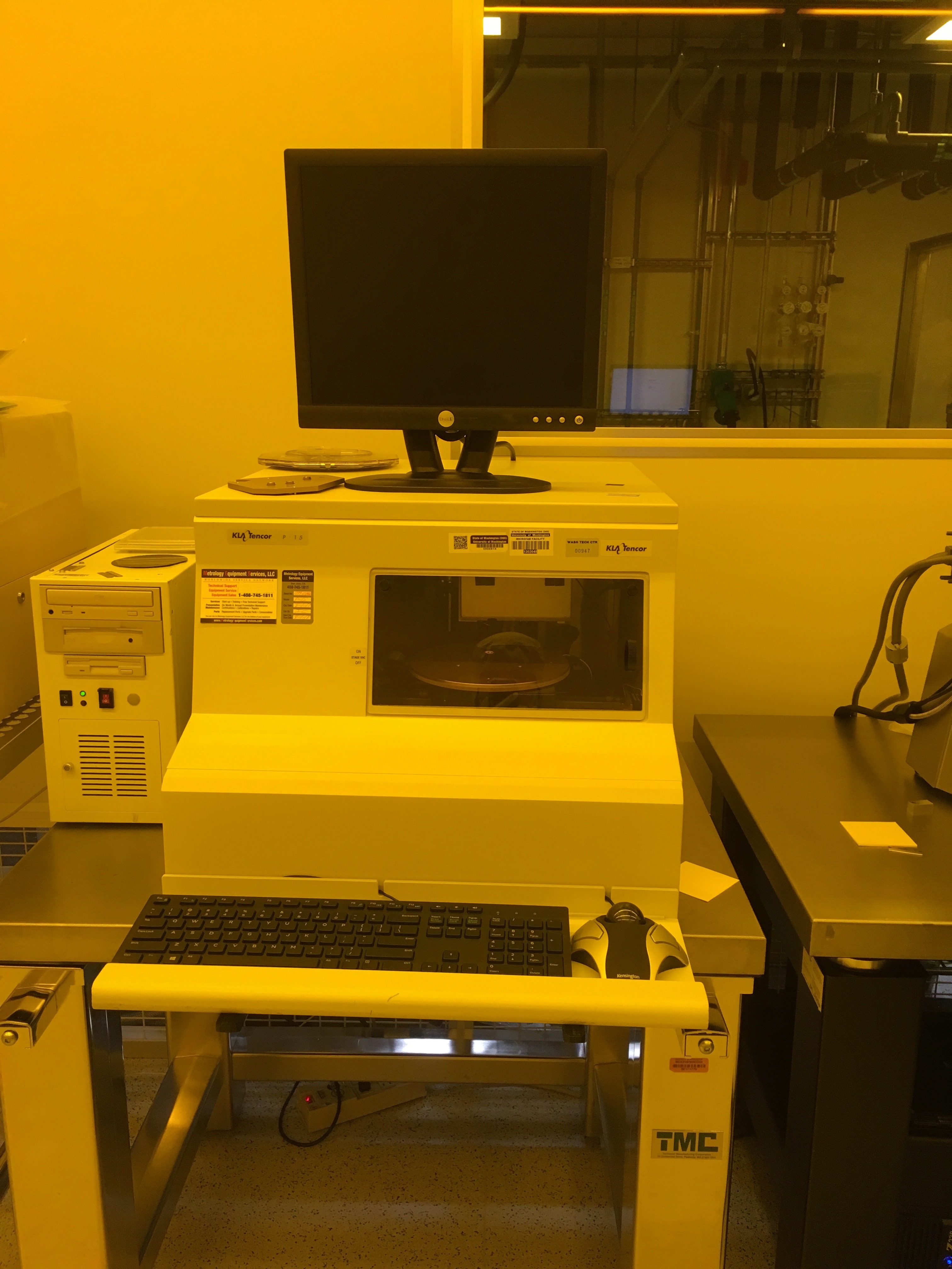
KLA Tencor P15 Contact Profilometer
| Coral ID: | WNF--Profilometer--P15 |
| Manufacturer: | Tencor |
| Model: | P-15 |
| Lab: | WNF |
| Area: | Device and Structure Characterization |
| Manual: | https://www.coral.washington.edu/upload/manuals/P15.pdf |
| UW Academic Rate: | $55/hr |
| Industrial Rate: | $165/hr |
| Outside Academic Rate: | $55/hr |
Description
A surface profilometer for physical measurement of topography on wafers. Can program a sequence of locations to scan, providing 2-D and pseudo-3-D measurement of topography, as well as calculation of film stress. Step heights down to tens of nanometers are possible.
Details
(none given)
Materials Restrictions
(none)
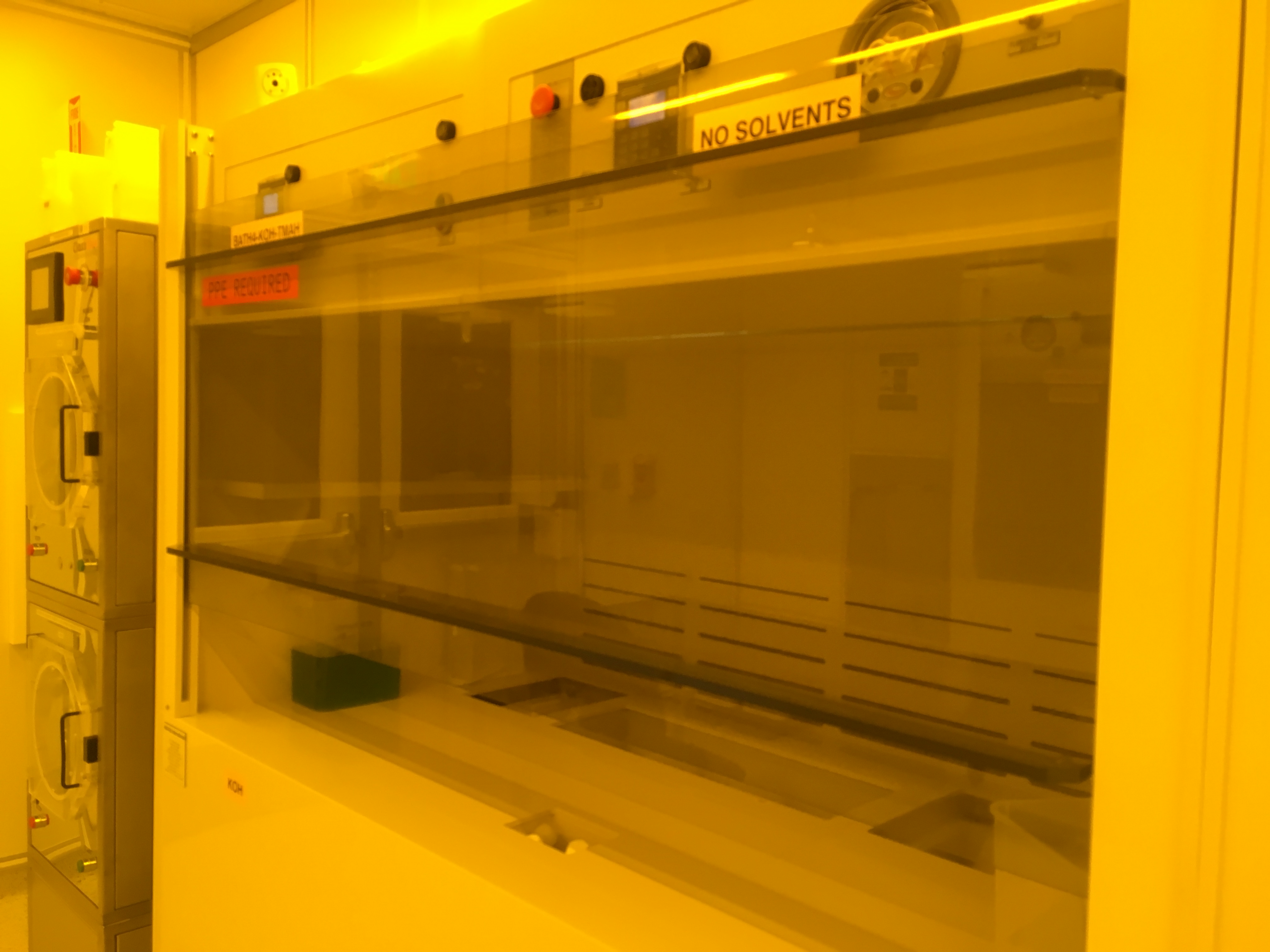
KOH-TMAH Station
| Coral ID: | WNF--BATH4-KOH-TMAH |
| Manufacturer: | WAFAB International |
| Model: | 72" Front Access Wet Bench (KOH/TMAH Station) |
| Lab: | WNF |
| Area: | Wet Etch and Cleaning |
| Manual: | https://www.coral.washington.edu/upload/manuals/KOH_TMAH_Sept2022.pdf |
Description
Wet bench with dedicated baths that can be used for KOH and TMAH.
Details
Both baths KOH. Please contact staff if TMAH processing is needed. Baths can be refilled by request
Materials Restrictions
(none)
Kratos Axis Ultra DLD X-ray Photoelectron Spectrometer
| Coral ID: | SARC--Kratos |
| Manufacturer: | Kratos |
| Model: | Axis Ultra DLD |
| Lab: | MAF |
| Area: | Thin Film and Materials Characterization |
| UW Academic Rate: | $48/hr |
| Industrial Rate: | $248/hr |
| Outside Academic Rate: | $58/hr |
Description
X-ray Photoelectron Spectroscopy (XPS) (which is also known as ESCA) exploits the photoelectric effect to obtain information about the chemical composition of a surface. XPS can identify all elements (except H and He) present in the outermost 10 nm of a surface that are in concentrations greater than 0.1 atomic %. The elemental composition of a surface can be quantified (±10% or better). High-resolution XPS spectra can provide information about the molecular environment of a particular element (oxidation state, bonding atoms, etc.) Since the major components of the XPS systems are under computer control, automated data acquisition is possible allowing the instrument to be used 24/7.
Details
The instrument is equipped with a monochromatic Al Kα x-ray source as well as non-monochromatic Al and Mg sources. Typically a 700x300 micron spot on the sample is analyzed, but the spot sizes can be decreased down to ~100 microns. Samples up to 1 x 9 cm can be measured. Special capabilities of the Kratos Axis Ultra DLD include ultraviolet photoelectron spectroscopy (UPS), XPS imaging, depth profiling using monoatomic argon, and non-destructive depth profiling of the outer 10 nm using angle-resolved XPS
Materials Restrictions
(none)
Lapping/Polishing Station
| Coral ID: | MAF--Grinder-Polisher--Maopa-XP8 |
| Manufacturer: | Maopa |
| Model: | XP-8 |
| Lab: | MAF |
| UW Academic Rate: | $34/hr |
| Industrial Rate: | $126/hr |
| Outside Academic Rate: | $40/hr |
Description
8" manual polishing station
Details
(none given)
Materials Restrictions
(none)
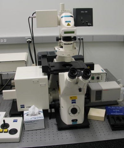
Laser Confocal Microscope
| Coral ID: | MAF--Confocal-Microscope--Zeiss-LSM-510 |
| Manufacturer: | Zeiss |
| Model: | LSM 510 |
| Lab: | MAF |
| Area: | Inspection |
| UW Academic Rate: | $34/hr |
| Industrial Rate: | $126/hr |
| Outside Academic Rate: | $40/hr |
Description
Confocal microscope for Z sectioning by laser scanning samples; Excitation at 458,477,488,514,543, and 643nm
Details
(none given)
Materials Restrictions
No BSL2. Discuss samples with staff
Leica DVM2500 digital microscope
| Coral ID: | WNF--Microscope--Leica-Backend |
| Manufacturer: | Leica |
| Model: | DVM2500 |
| Lab: | WNF |
| Area: | Inspection |
| UW Academic Rate: | $11/hr |
| Industrial Rate: | $33/hr |
| Outside Academic Rate: | $11/hr |
Description
This digital microscope is capable of variable angles, has a long working distance, and has magnification from 20x to 160x,
Details
(none given)
Materials Restrictions
(none)
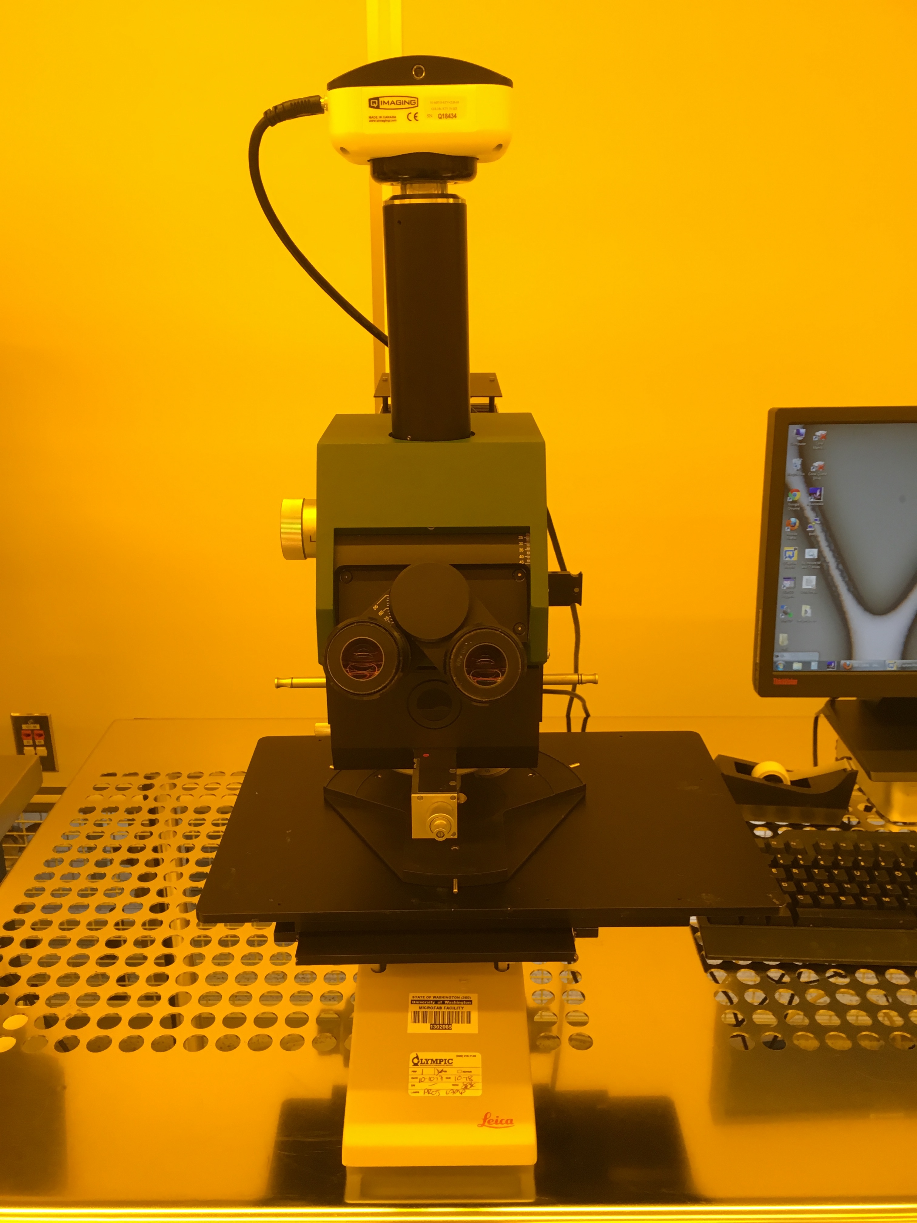
Leica Microscope
| Coral ID: | WNF--Microscope--Leica |
| Manufacturer: | Leica / Reichert |
| Model: | Polylite 88 |
| Lab: | WNF |
| Area: | Inspection |
| UW Academic Rate: | $11/hr |
| Industrial Rate: | $33/hr |
| Outside Academic Rate: | $11/hr |
Description
Priority inspection in support of wet chemistry and develop activities. NO WET MATERIALS ARE ALLOWED ON THE MICROSCOPE STAGE.
Microscope is not interlocked for ease of use. Users are expected to be logged into Wet Chem Bay A to use this asset.
Camera computer is interlocked in CORAL. Users undertaking dedicated inspection activities longer than 5-10 minutes should be logged into CORAL (not Bay A)
The microscope is capable of Nomarski imaging/DIC and has a stage that can accommodate wafers up to 150 mm.
Details
(none given)
Materials Restrictions
No Wet Materials allowed on Microscope Stage
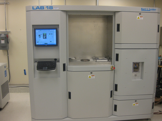
Lesker Sputter
| Coral ID: | WNF--SPUT03--Lesker |
| Manufacturer: | Lesker |
| Model: | Lab 18 |
| Lab: | WNF |
| Area: | Thin Film Processing |
| Manual: | https://www.coral.washington.edu/upload/manuals/SPUT03 Lesker Sputter - SOP.pdf |
| UW Academic Rate: | $77/hr |
| Industrial Rate: | $231/hr |
| Outside Academic Rate: | $77/hr |
Description
This cryo pumped system is used for sputter deposition of films, with DC, RF, and pulsed DC power supplies. Targets materials include: Al, Ti, Au, Ti/W, Ni, ZnO, ITO, Nb, Cr, Cu, Ir, and Ni/Cr.
Details
Three sample holders are available for the system. There are holders for both 150mm and 4 inch wafers, plus a reconfigurable small-parts holder. Small parts must be of similar thickness to a wafer. Additional holders for specific samples can be fabricated.
The system has four power supplies. Power supply 1 (1500W max, DC) can be connected to guns 1, 2, 3, and 4. Power supply 4 (600W max, RF) can be connected to all five guns. Power supply 5 (1500W max, DC/pulsed DC) connects only to gun 5. Power supply 6 (100W max, RF) is used to bias the substrate. Only one power supply can connected to each gun at one time. Up to three guns can be sputtering at the same time if the guns are chosen carefully e.g. Gun 1 (DC), Gun 3 (RF), Gun 5 (DC) could be used for cosputtering.
Radio frequency (RF) supplies are used to counteract charge buildup that occurs on nonconducting targets. This is required for most oxides and nitrides used in the system. Conductive samples can be sputtered using an RF supply, but tend to sputter more slowly than with DC supplies.
Materials Restrictions
Organic substrates require staff review and permission prior to use. Photoresists are allowed in the system. Target placement must be reserved in advance by contacting darick@uw.edu. The target schedule is available here: http://goo.gl/fd0Gbh
Life Canvas Light Sheet Microscope
| Coral ID: | Miscellaneous--LightSheetMicroscope--LifeCanvas-SmartSPIM |
| Lab: | Miscellaneous |
| Area: | Inspection |
Description
Life Canvas Light Sheet Microscope. Resides in J182 of the NAPE Imaging and Neural Circuits Core
Details
(none given)
Materials Restrictions
(none)
Life Canvas Light Sheet Microscope Analysis
| Coral ID: | Miscellaneous--MicroscopeAnalysis-LifeCanvas-SmartSPIM |
| Lab: | Miscellaneous |
| Area: | Other |
Description
Life Canvas Light Sheet Microscope Analysis Computer. Resides in J182 of the NAPE Imaging and Neural Circuits Core
Details
(none given)
Materials Restrictions
(none)
Low-Speed Diamond Saw
| Coral ID: | MAF--Slow-Saw--Buehler-Isomet |
| Manufacturer: | Buehler |
| Model: | Isomet |
| Lab: | MAF |
| Area: | Packaging and Back End |
| UW Academic Rate: | $34/hr |
| Industrial Rate: | $126/hr |
| Outside Academic Rate: | $40/hr |
Description
Diamond wheel saw for trimming epoxy potted samples and hard materials.
Details
Water lubrication
Materials Restrictions
(none)
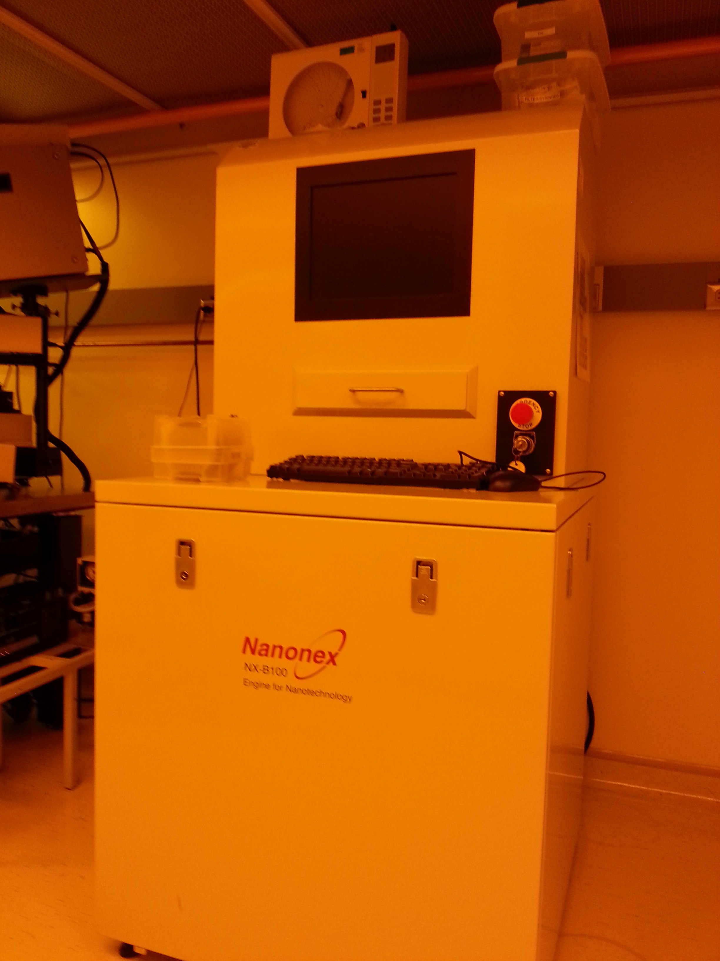
Nanoimprinting
| Coral ID: | WCET--Nanoimprint |
| Manufacturer: | Nanonex |
| Model: | NX-B100 |
| Lab: | WCET |
| Area: | Lithography and Direct Patterning |
| Manual: | https://www.coral.washington.edu/upload/manuals/SOP NIL NXB100v2.pdf |
| UW Academic Rate: | $50/hr |
| Industrial Rate: | $150/hr |
| Industrial Membership Rate: | $63/hr |
| Internal Rate: | $0/hr |
| Non-Profit Rate: | $0/hr |
| Outside Academic Rate: | $75/hr |
| Outside Academic Membership Rate: | $0/hr |
| UW Academic Membership Rate: | $0/hr |
Description
Thermal nanoimprinting of substrates up to 75mm.
Details
Please see the operating procedures above - this is actually two SOPs (the second beginning on page 7) written by WNF users - both are useful.
Materials Restrictions
typical mold/resist/substrate stacks should not be thicker than 2 mm however, thicker stacks are possible - please see tool owner
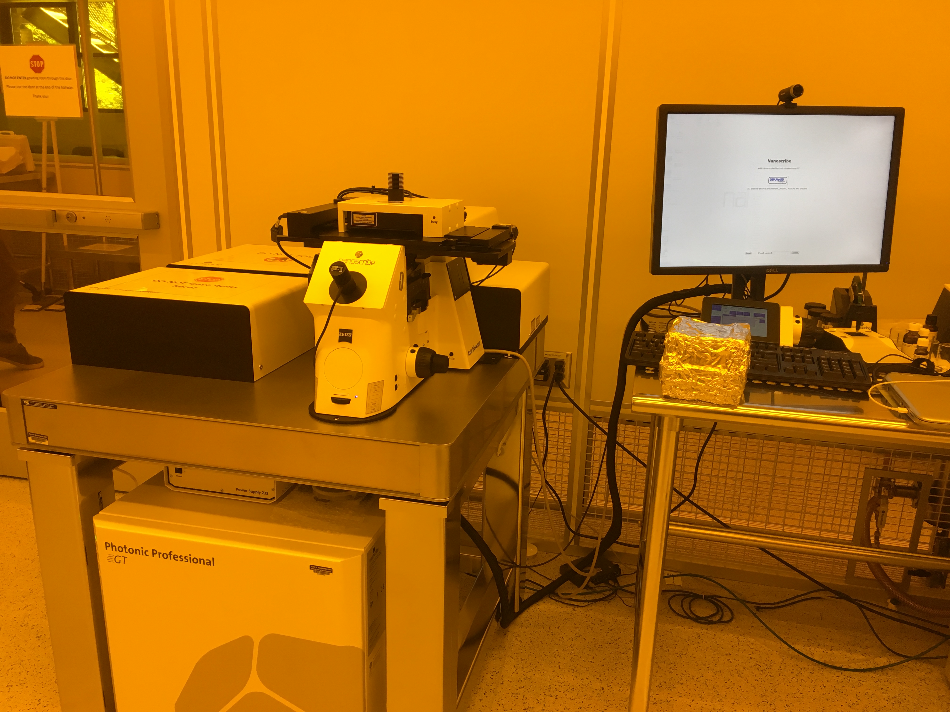
Nanoscribe Photonic Professional GT
| Coral ID: | WNF--Nanoscribe-Photonic-Professional-GT |
| Manufacturer: | Nanoscribe |
| Model: | Photonic Professional (GT) |
| Lab: | WNF |
| Area: | Lithography and Direct Patterning |
| Manual: | https://www.coral.washington.edu/upload/manuals/nanoscribe_sop_1.1.pdf |
| UW Academic Rate: | $33/hr |
| Industrial Rate: | $99/hr |
| Outside Academic Rate: | $33/hr |
Description
3D printing platform for micro- and nanofabrication demands utilizing two-photon polymerization. Structures can either be designed in 3D printer compatible CAD software programs or directly implemented in Nanoscribe’s GWL scripting language.
Details
(none given)
Materials Restrictions
(none)
Nikon 6" Microscope
| Coral ID: | WNF--Microscope08--Nikon |
| Manufacturer: | Nikon |
| Model: | LV150N |
| Lab: | WNF |
| Area: | Inspection |
| UW Academic Rate: | $11/hr |
| Industrial Rate: | $33/hr |
| Outside Academic Rate: | $11/hr |
Description
This is one of the primary imaging optical microscopes at the WNF. It includes five objectives (5X - 100X), an LED light source, a UV cutoff filter, and imaging in both bright field and dark field. It is capable of imaging clean samples as small as chips and as large as 150 mm wafers.
Details
(none given)
Materials Restrictions
(none)
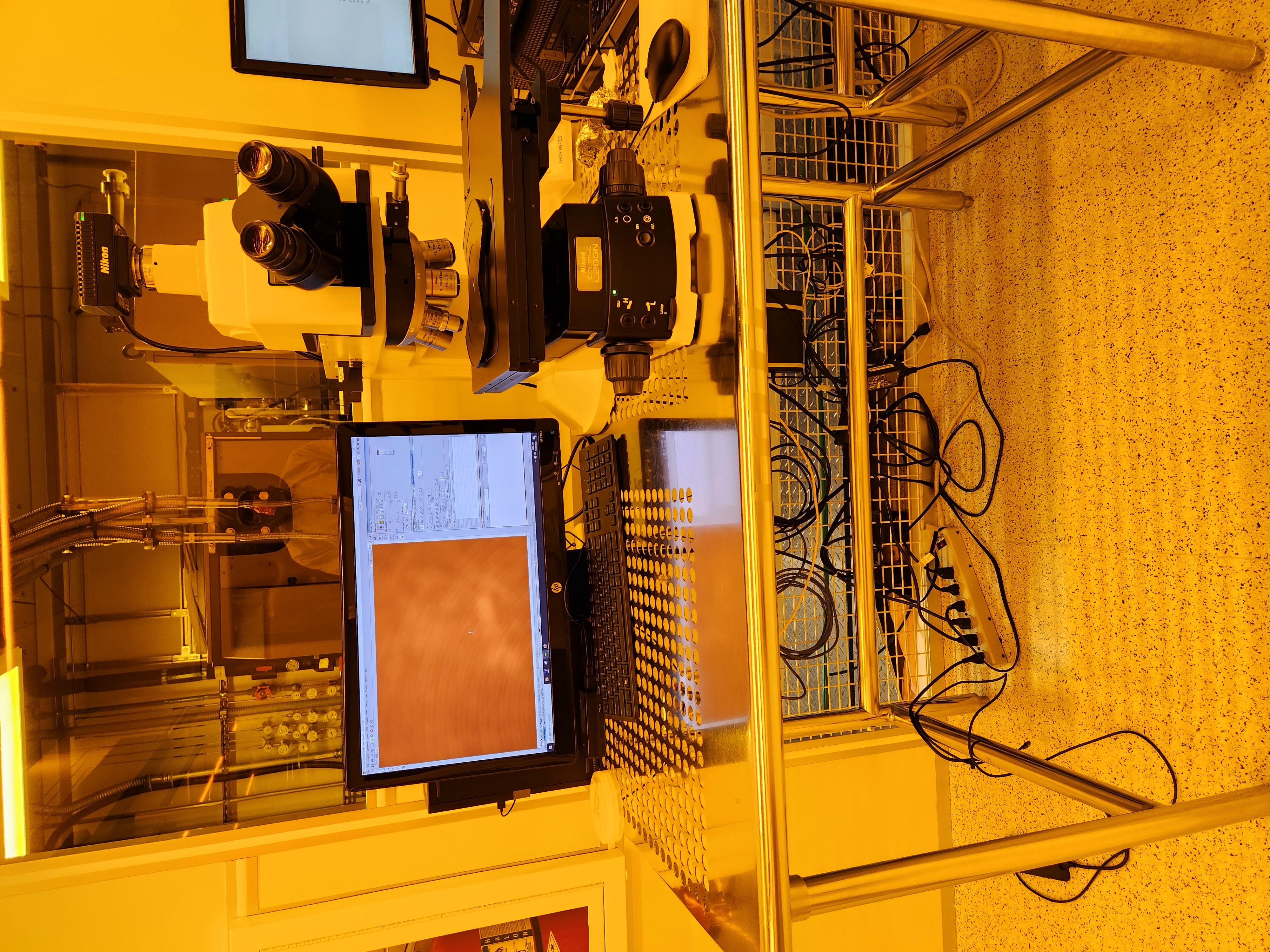
Nikon 8" Imaging Microscope
| Coral ID: | WNF--Microscope09--Nikon |
| Manufacturer: | Nikon |
| Model: | Eclipse L200ND |
| Lab: | WNF |
| Area: | Inspection |
| UW Academic Rate: | $11/hr |
| Industrial Rate: | $33/hr |
| Outside Academic Rate: | $11/hr |
Description
This is the primary optical microscope for imaging of wafers at the WNF. It includes six objectives (2.5X - 100X), an LED light source, a UV cutoff filter, bright field and dark field imaging, and differential interference contrast. It is capable of imaging clean samples as small as chips and as large as 200 mm wafers.
Details
(none given)
Materials Restrictions
Clean and dry samples only. Resists must be properly baked. Nothing should be left behind on the stage after inspection.
Nikon Semiconductor Optical Microscope
| Coral ID: | WNF--Microscope--Nikon |
| Manufacturer: | Optiphot |
| Model: | 200 |
| Lab: | WNF |
| Area: | Inspection |
| Manual: | https://www.coral.washington.edu/upload/manuals/201309 Nikon Microscope.pdf |
| UW Academic Rate: | $11/hr |
| Industrial Rate: | $33/hr |
| Outside Academic Rate: | $11/hr |
Description
This optical microscope including dark-field imaging, LED light sources for both reflected and transmitted illumination, and a camera for image capture. The stage can accommodate wafers up to 200 mm in diameter as well as irregular samples.
Details
(none given)
Materials Restrictions
(none)
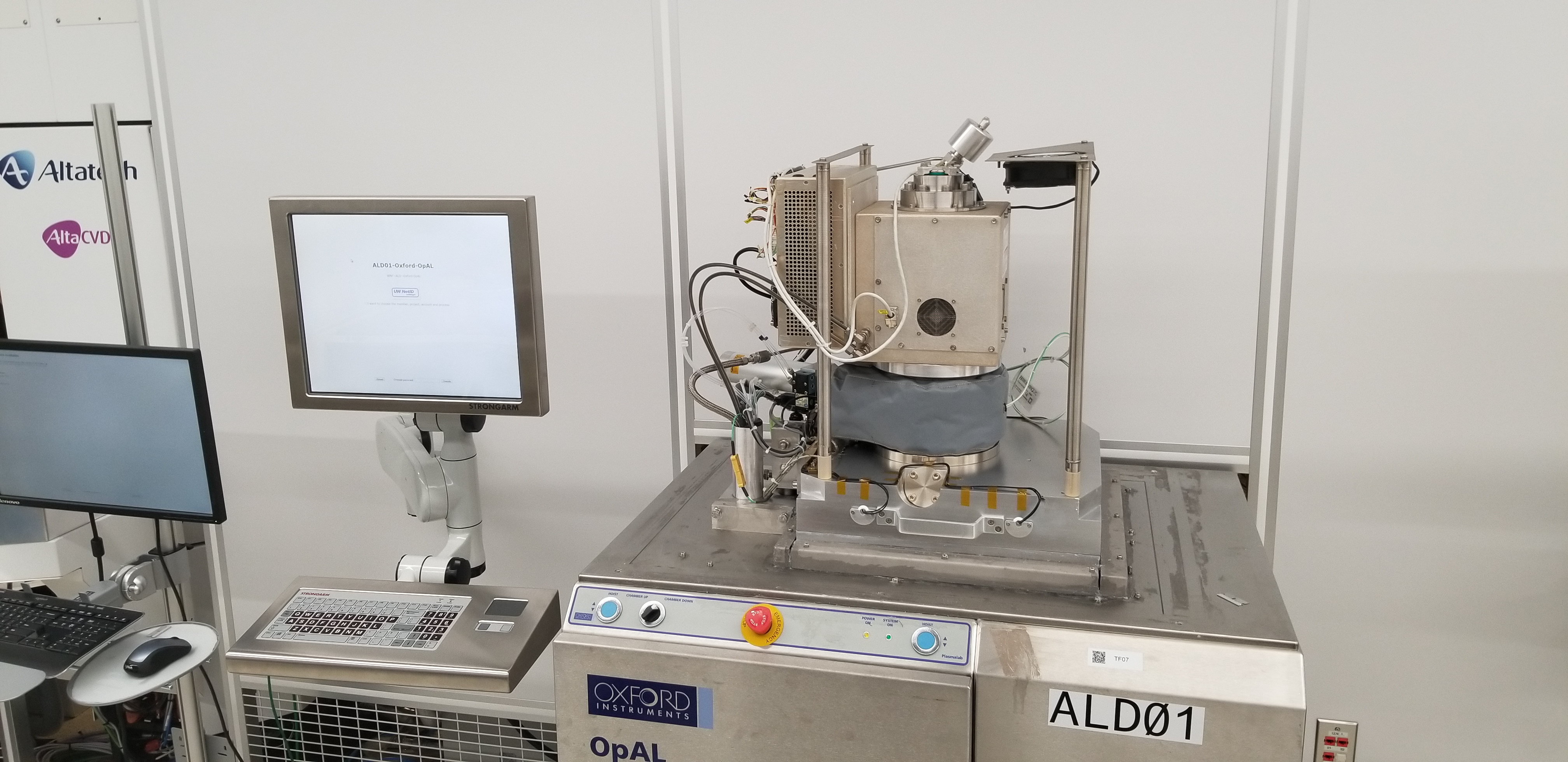
Oxford OpAL ALD
| Coral ID: | WNF--ALD--Oxford-OpAL |
| Manufacturer: | Oxford Instruments |
| Model: | Plasmalab 80Plus OpAL ALD |
| Lab: | WNF |
| Area: | Thin Film Processing |
| Manual: | https://www.coral.washington.edu/upload/manuals/ALD01 SOP 20221129.pdf |
| UW Academic Rate: | $77/hr |
| Industrial Rate: | $231/hr |
| Outside Academic Rate: | $77/hr |
Description
This atomic layer deposition (ALD) system deposits layers of material monolayer by monolayer. Presently available: Al2O3 and HfO2.
TMA: trimethyl alumiminum
TEMAH: tetrakis(ethylmethylamino) hafnium
Details
This system provides precise growth control over thin films. Layers have been used as dielectrics and mask layers. Processes can be run in either the plasma-ALD or thermal-ALD modes. Al2O3 run temperatures range from 50C to 300C. HfO2 from 200C to 290C.
Materials Restrictions
This system can accommodate up to 200mm wafers. The chamber opens for loading so numerous smaller pieces can be arranged inside the system.
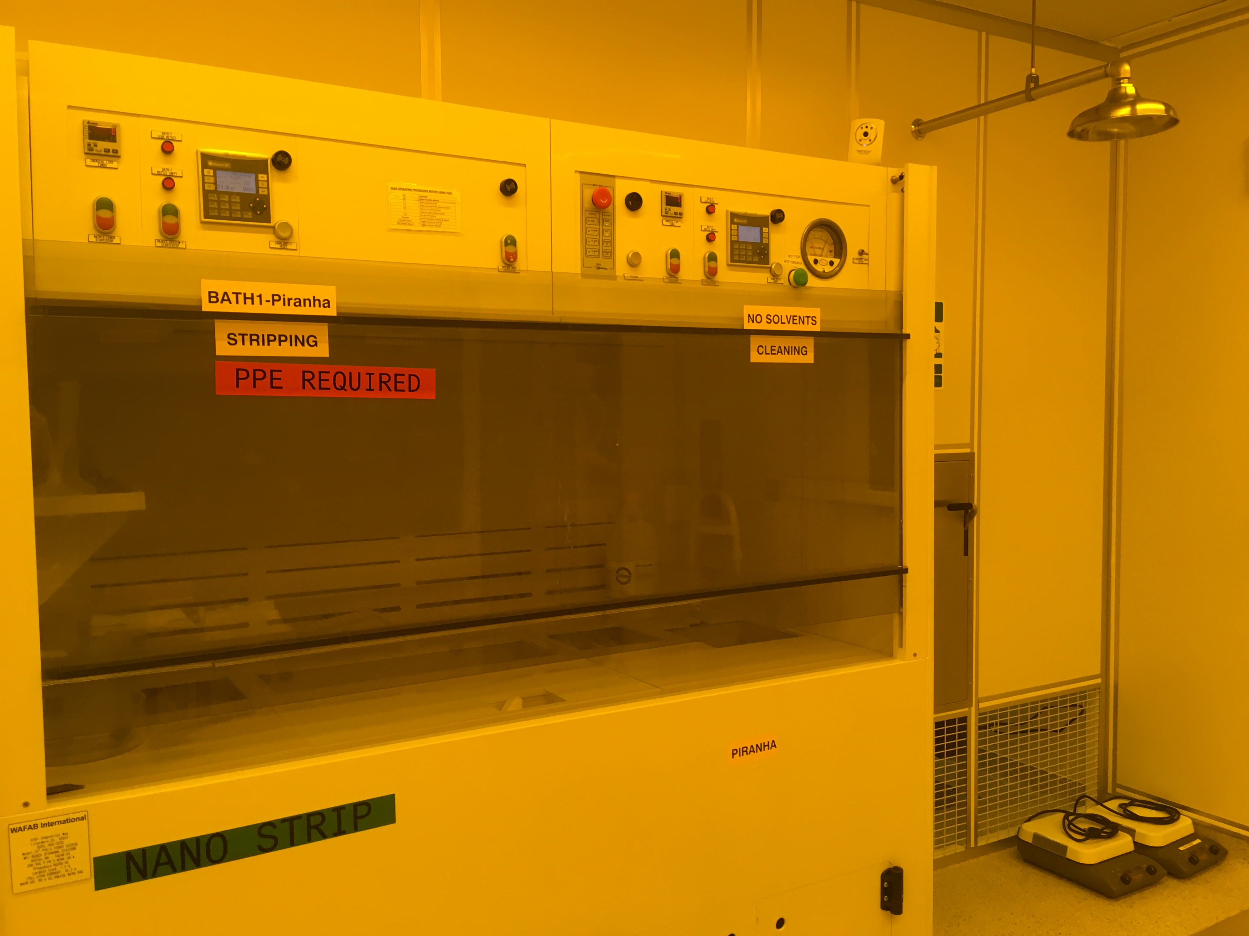
Piranha Wet Bench
| Coral ID: | WNF--BATH1-Piranha |
| Manufacturer: | WAFAB International |
| Model: | 72" PVC-C Front Access Wet Bench (Piranha Station) |
| Lab: | WNF |
| Area: | Wet Etch and Cleaning |
| Manual: | https://www.coral.washington.edu/upload/manuals/BATH1-Piranha_2.0.pdf |
Description
Wet bench with dedicated baths for piranha and Nanostrip
Details
Piranha changed monthly
Materials Restrictions
(none)
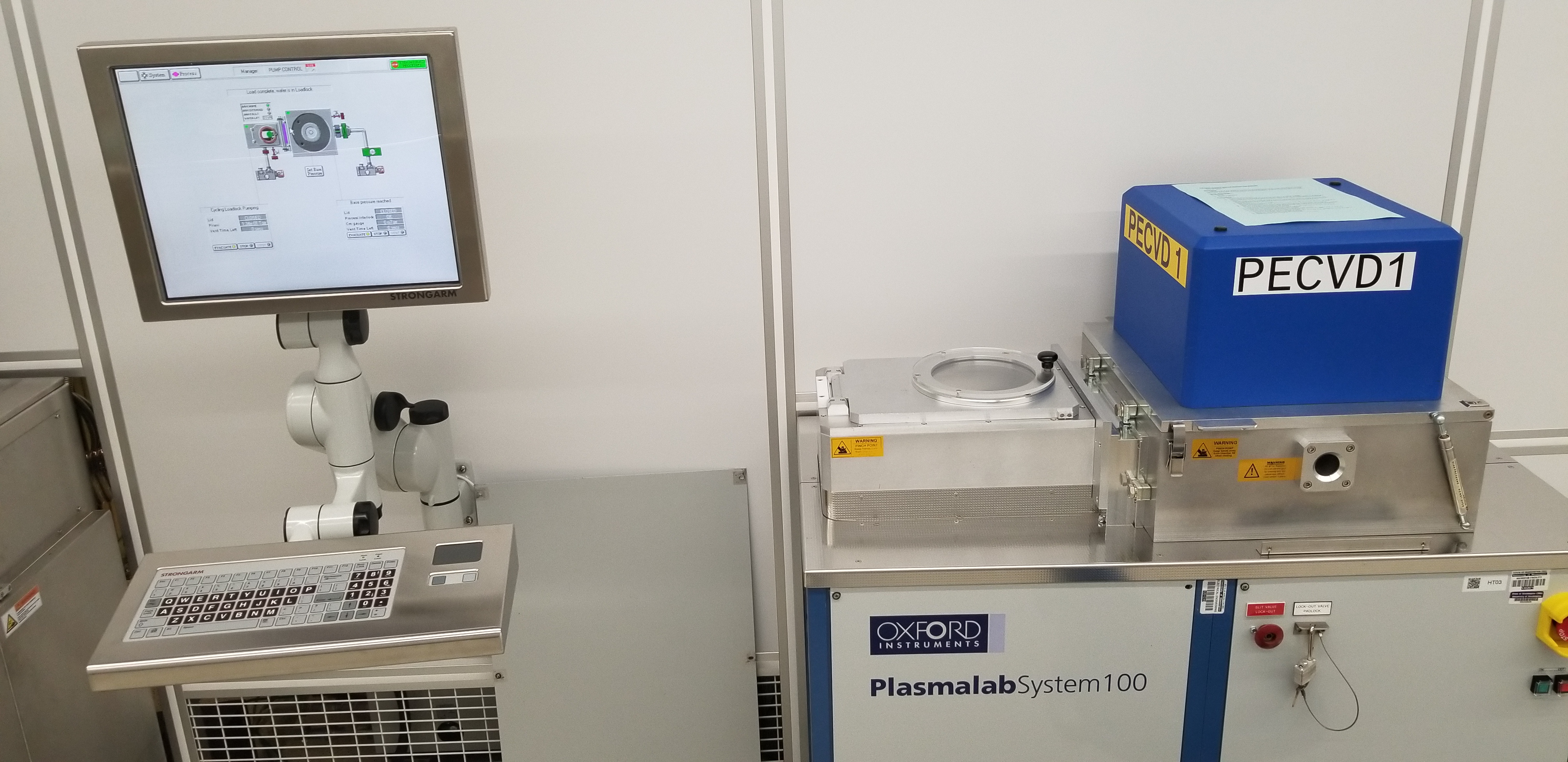
Plasma Enhanced CVD
| Coral ID: | WNF--PECVD1-Oxford |
| Manufacturer: | Oxford Instruments |
| Model: | Plasma Lab 100 |
| Lab: | WNF |
| Area: | Thin Film Processing |
| Manual: | https://www.coral.washington.edu/upload/manuals/PECVD1-SOP.pdf |
| UW Academic Rate: | $55/hr |
| Industrial Rate: | $165/hr |
| Outside Academic Rate: | $55/hr |
Description
Plasma-Enhanced Chemical Vapor Deposition (PECVD) of Silicon Dioxide, Silicon Nitride, Silicon Oxynitride and amorphous silicon.
Details
Wafers up to 8in. Smaller chips can be accomodated using a 100mm silicon wafer as a carrier wafer.
Materials Restrictions
Samples going into the chamber must not contaminate the chamber or contain materials that will decompose at 350C.
Polos Spin Developer
| Coral ID: | WNF--SPIN06--Matthews-Develop |
| Manufacturer: | Polos |
| Model: | 200 |
| Lab: | WNF |
| Area: | Lithography and Direct Patterning |
| Manual: | https://www.coral.washington.edu/upload/manuals/Spray Develop Tool SOP - Public.docx |
| UW Academic Rate: | $11/hr |
| Industrial Rate: | $33/hr |
| Outside Academic Rate: | $11/hr |
Description
This spin developer is setup to automatically develop using AD10. This equipment is not owned by the WNF; please contact the tool owner for additional information.
Details
(none given)
Materials Restrictions
(none)
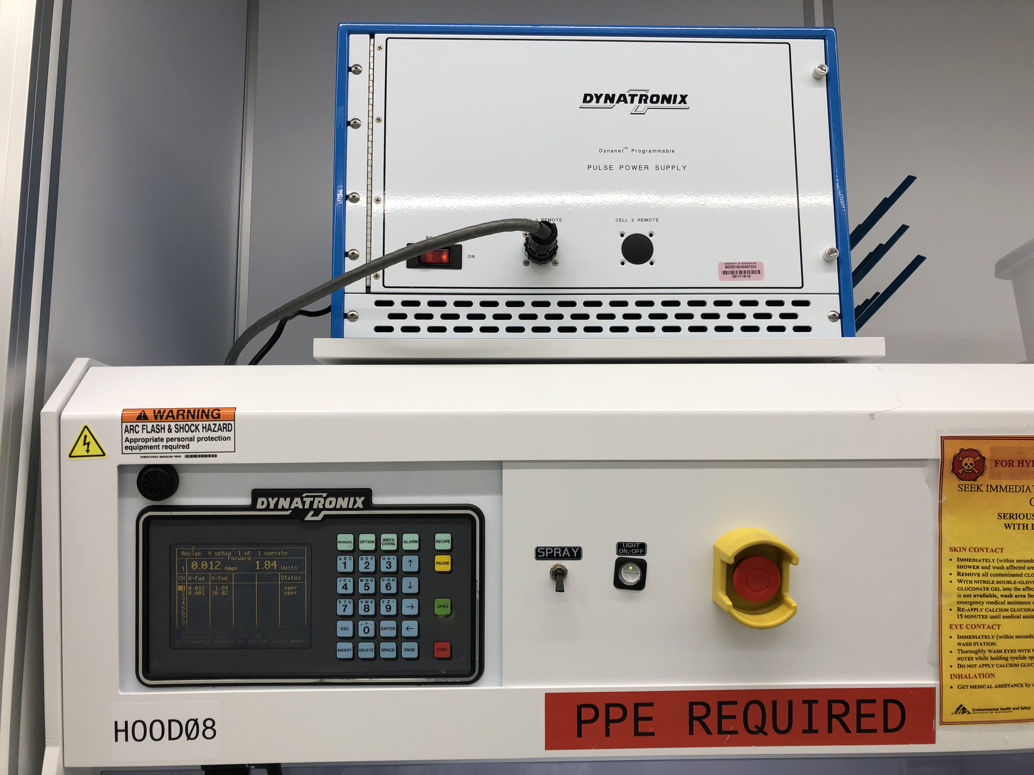
Pulse Power Supply
| Coral ID: | WNF--PPS |
| Manufacturer: | Dynatronix |
| Lab: | WNF |
| Area: | Thin Film Processing |
| Manual: | https://www.coral.washington.edu/upload/manuals/Pulse Power Suppy 20210728.pdf |
| UW Academic Rate: | $11/hr |
| Industrial Rate: | $33/hr |
| Outside Academic Rate: | $11/hr |
Description
Pulsed power supply for general electrodeposition processes.
This unit had originally been located in HOOD08 but was moved to HOOD10 when the GoldBath power supply failed.
Since HOOD08 has no designated power supply the electrode leads for the PPS must be plugged to the banana cable receptacles in HOOD10.
Details
(none given)
Materials Restrictions
(none)
 (2).JPG)
Rapid Thermal Annealer
| Coral ID: | WNF--RTA-Clean |
| Manufacturer: | Allwin32 |
| Model: | AccuThermo AW 610 |
| Lab: | WNF |
| Area: | Thin Film Processing |
| Manual: | https://www.coral.washington.edu/upload/manuals/RTA SOP 20171023.pdf |
| UW Academic Rate: | $55/hr |
| Industrial Rate: | $165/hr |
| Outside Academic Rate: | $55/hr |
Description
Rapid thermal annealer
Details
Clean system isolation tube: 1119-16518 Clean system quartz tray: 1119-16534 General system isolation tube 1117-15748 General system quartz tray: 1210-13236 Backup set isolation tube: 819-16467 Backup set quartz tray: 1119-16531
Materials Restrictions
(none)
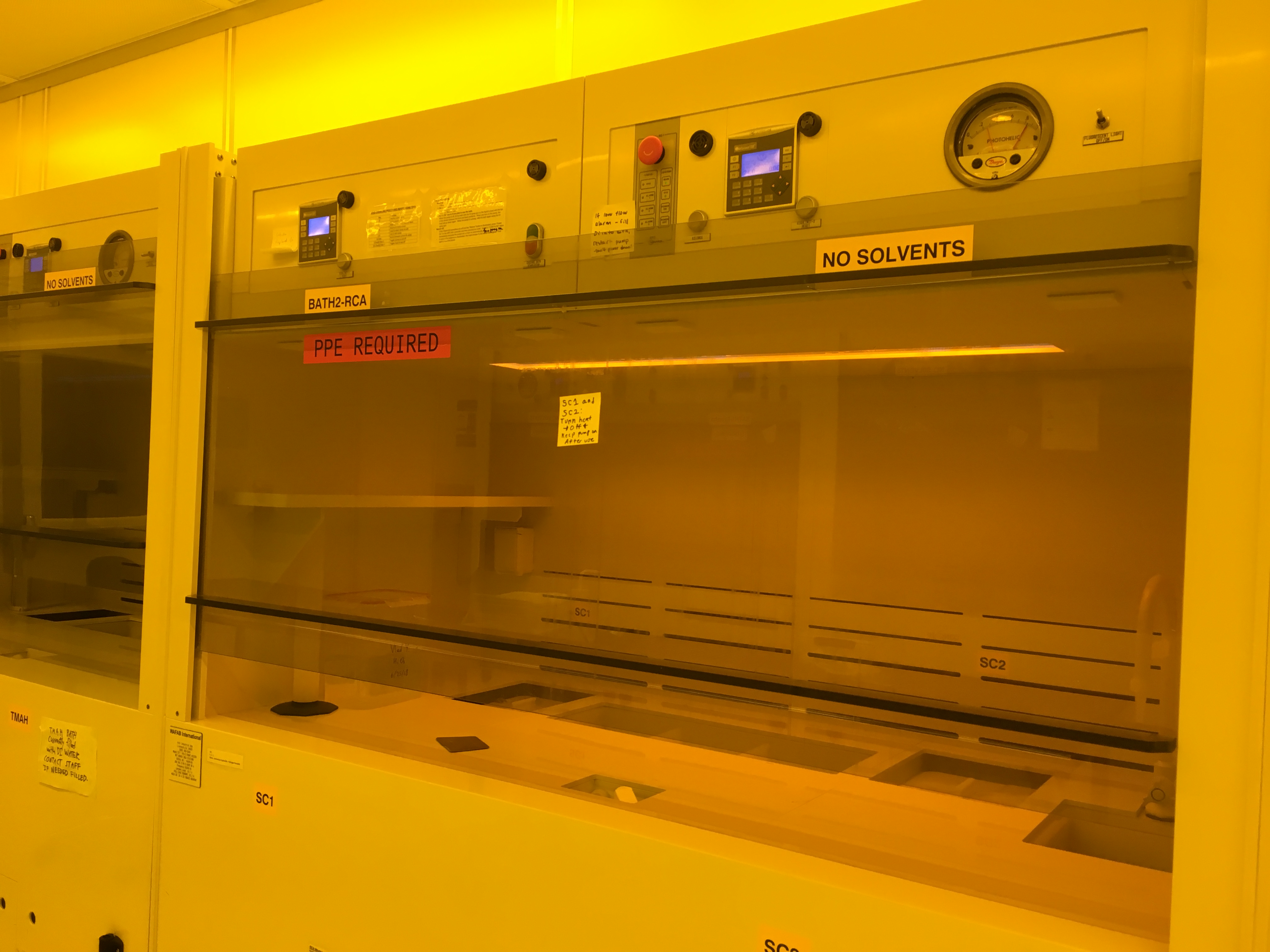
RCA Station:
| Coral ID: | WNF--BATH2-RCA |
| Manufacturer: | WAFAB International |
| Model: | 72" PVC-C Front Access Wet Bench (RCA Station) |
| Lab: | WNF |
| Area: | Wet Etch and Cleaning |
| Manual: | https://www.coral.washington.edu/upload/manuals/BATH2-RCA_2.0.pdf |
Description
Wet bench dedicated to RCA Standard Clean 1 (SC1) and Standard Clean 2 (SC2)
Details
Turn on Heaters to reach operating temperature of 80C. Be sure to turn off heaters after use.
Baths Refilled upon Request. See Lab Status for latest Date.
SC1 (5:1:1 H2O:NH4OH:H2O2) -- Recommended change weekly.
SC2 (5:1:1 H2O:HCl:H2O2) -- Recommended change monthly
Materials Restrictions
(none)
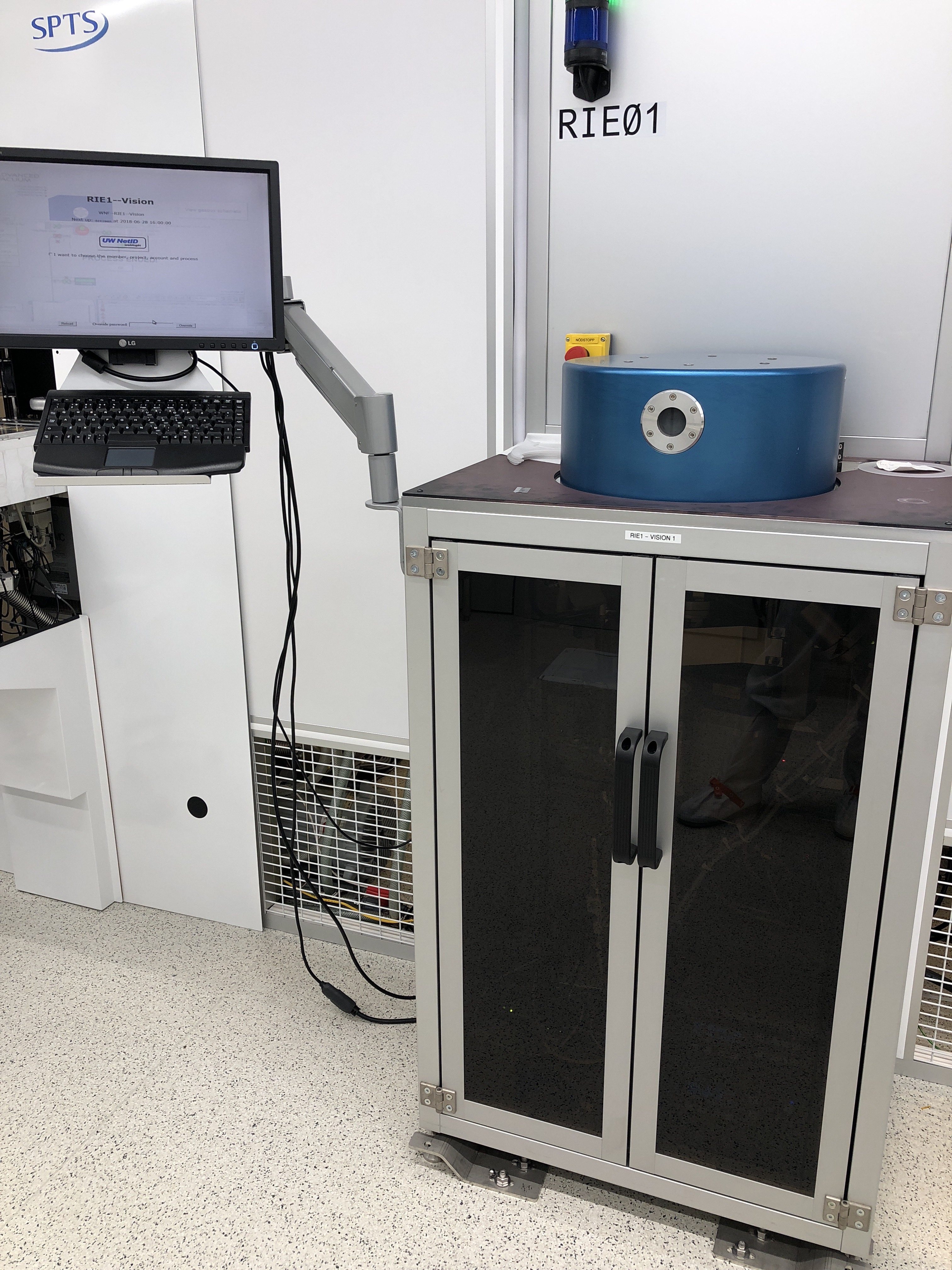
Reactive Ion Etcher 1
| Coral ID: | WNF--RIE1--Vision |
| Manufacturer: | Vision |
| Model: | Vision 320 RIE Mark II |
| Lab: | WNF |
| Area: | Dry Etch |
| Manual: | https://www.coral.washington.edu/upload/manuals/RIE1-Cortex_UserManual_v5.1.pdf |
| UW Academic Rate: | $77/hr |
| Industrial Rate: | $231/hr |
| Outside Academic Rate: | $77/hr |
Description
A parallel-plate Reactive Ion Etch (RIE) system. Open load for flexible substrate handling. Etch gases are: Ar, CF4, CHF3, O2, and SF6.
Details
Open load with ~12-inch platen allowing multiple substrates and substrate sizes.
Materials Restrictions
Allowed Etch target materials: silicon, silicon nitride, silicon oxide, PMDS, Polyimide, Parylene, Graphene, photoresist. Allowed mask materials: photoresist, ebeam-resist, silicon oxide, silicon nitride, alumina. No metal masks are allowed. No Exposed metal (including copper, gold, and silver) nor dirty glasses (<99% SiO2). Please contact the tool owner to discuss materials not included on this list. No high-vapor-pressure materials.
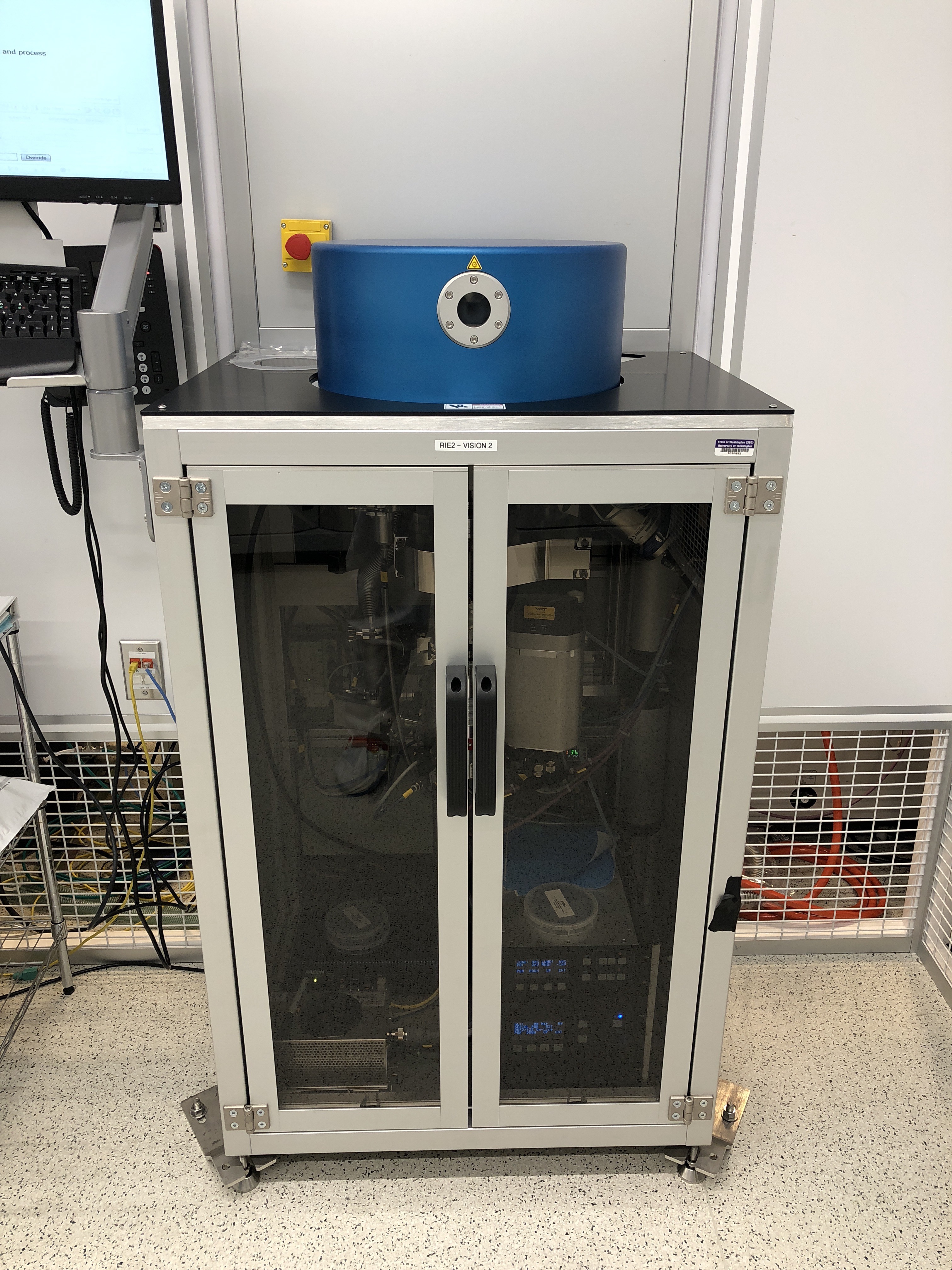
Reactive Ion Etcher 2
| Coral ID: | WNF--RIE2--Vision |
| Manufacturer: | Advanced Vacuum |
| Model: | Vision 320 MkII |
| Lab: | WNF |
| Area: | Dry Etch |
| Manual: | https://www.coral.washington.edu/upload/manuals/RIE2-Cortex_UserManual_v3.1.pdf |
| UW Academic Rate: | $77/hr |
| Industrial Rate: | $231/hr |
| Outside Academic Rate: | $77/hr |
Description
A parallel-plate Reactive Ion Etch (RIE) system. Open load for flexible substrate handling. Etch gases are: Ar, CF4, CHF3, N2, O2, and SF6. This the designated clean RIE tool - Allowed materials are strictly enforced.
Details
Open load system with 12-inch platen allowing multiple substrates and substrate sizes.
Materials Restrictions
Allowed Etch target materials: silicon, silicon nitride, silicon oxide, PMDS, Polyimide, Parylene, Graphene, photoresist. Allowed mask materials: photoresist, ebeam-resist, silicon oxide, silicon nitride, alumina. No metal masks are allowed. No Exposed metal (including copper, gold, and silver) nor dirty glasses (<99% SiO2). Please contact the tool owner to discuss materials not included on this list. No high-vapor-pressure materials.
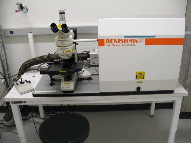
Renishaw Raman Confocal
| Coral ID: | MAF--Raman-Microscope--Renishaw-InVia |
| Manufacturer: | Renishaw |
| Model: | InVia |
| Lab: | MAF |
| Area: | Thin Film and Materials Characterization |
| UW Academic Rate: | $34/hr |
| Industrial Rate: | $126/hr |
| Outside Academic Rate: | $40/hr |
Description
Raman spectrometer with confocal microscope for characterization of bulk and nanoscale samples.
Details
Laser sources include 514 nm and 784 nm. Automated sample stage. CCD detection.
Materials Restrictions
Currently no restrictions.

Rite Track Automated Coater
| Coral ID: | WNF--Coater--Rite-Track-SVG90S |
| Manufacturer: | Rite Track |
| Model: | SVG-90S |
| Lab: | WNF |
| Area: | Lithography and Direct Patterning |
| Manual: | https://www.coral.washington.edu/upload/manuals/Rite Track SVG90S SOP.pdf |
| UW Academic Rate: | $77/hr |
| Industrial Rate: | $231/hr |
| Outside Academic Rate: | $77/hr |
Description
Automated coater cluster tool with 100mm, 150mm and 200mm capability. Auto dispenses AZ1512, AZ10XT, AZ701 and NR-9 3000 photoresists. Recipes often utilize frontside and backside EBR. Modules include: HMDS vapor prime, coater, cold plate and two vacuum bake ovens.
Details
(none given)
Materials Restrictions
(none)
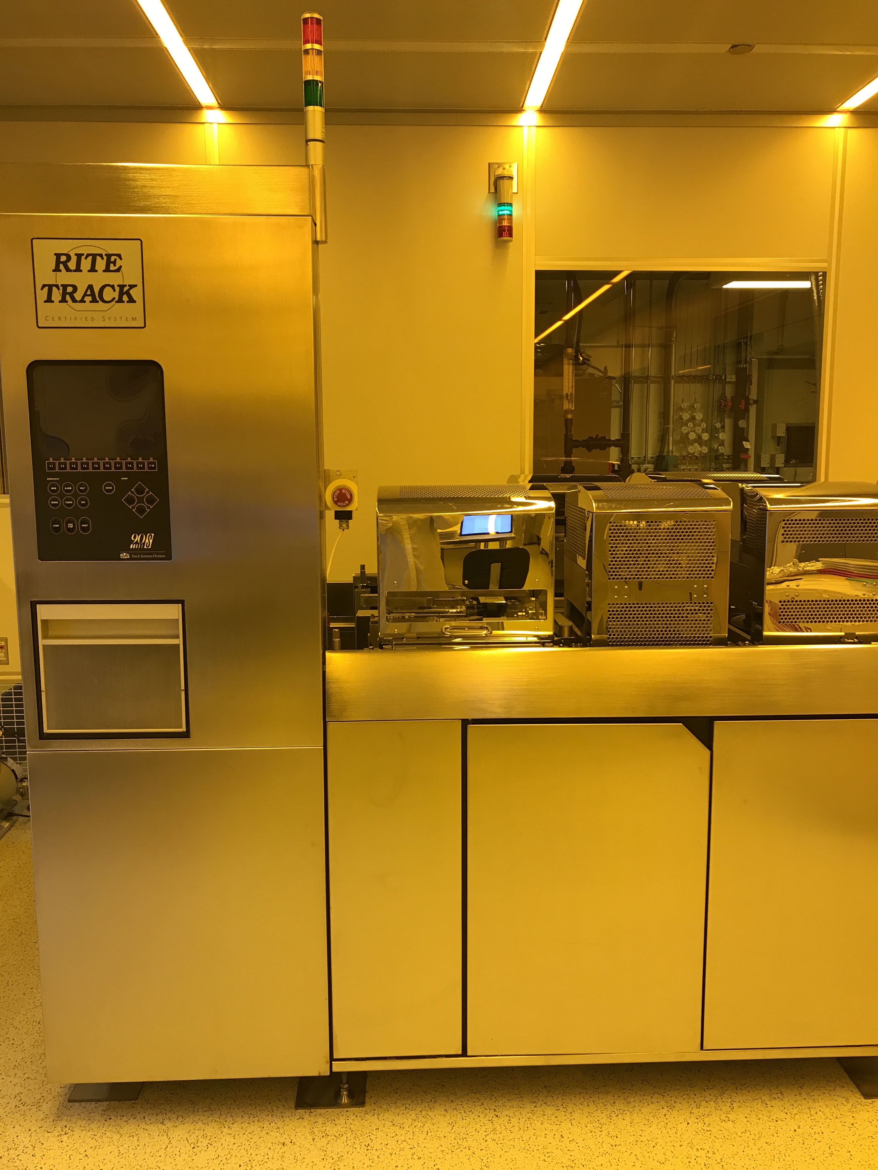
Rite Track Automated Developer
| Coral ID: | WNF--Developer--Rite-Track-SVG90S |
| Manufacturer: | Rite Track |
| Model: | SVG-90S |
| Lab: | WNF |
| Area: | Lithography and Direct Patterning |
| Manual: | https://www.coral.washington.edu/upload/manuals/Rite Track SVG90S SOP.pdf |
| UW Academic Rate: | $77/hr |
| Industrial Rate: | $231/hr |
| Outside Academic Rate: | $77/hr |
Description
Automated developer cluster tool with 100mm, 150mm and 200mm capability. Auto dispenses AD10MIF and AZ400K developers. Recipes utilize frontside and backside DI water rinse. Modules include: vacuum bake, cold plate, developer.
Details
(none given)
Materials Restrictions
(none)
SCS Labcoter Parylene Deposition System
| Coral ID: | WNF--Parylene |
| Manufacturer: | SCS |
| Model: | Labcoter |
| Lab: | WNF |
| Area: | Thin Film Processing |
| Manual: | https://www.coral.washington.edu/upload/manuals/Parylene Coater SOP.pdf |
| UW Academic Rate: | $33/hr |
| Industrial Rate: | $99/hr |
| Outside Academic Rate: | $33/hr |
Description
The Labcoter is a parylene coating system used to cover samples with a conformal layer of parylene-c.
Details
(none given)
Materials Restrictions
(none)
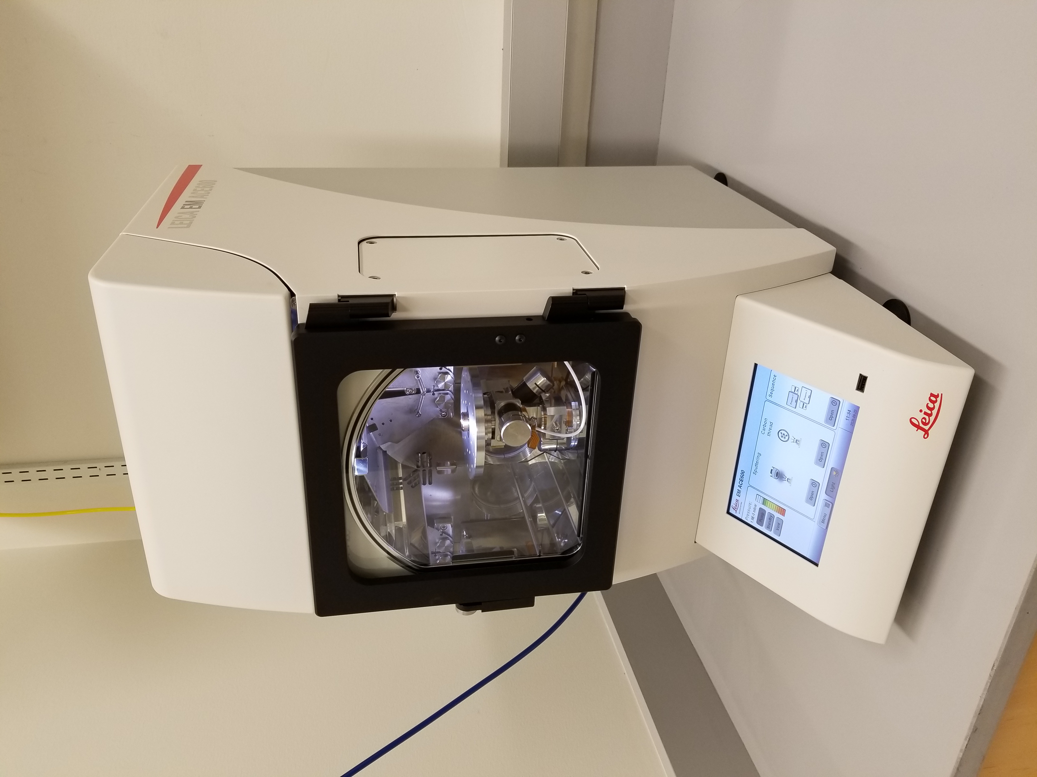
SEM Sample Coater
| Coral ID: | MAF--Coater--Leica-ACE600 |
| Manufacturer: | Leica |
| Model: | EM ACE600 |
| Lab: | MAF |
| Area: | Other |
| Manual: | https://www.coral.washington.edu/upload/manuals/Leica-coater-instructions.pdf |
| UW Academic Rate: | $0/hr |
| Industrial Rate: | $0/hr |
| Outside Academic Rate: | $0/hr |
Description
The Leica EM ACE600 is a sample preparation tool that applies conductive coatings to SEM samples prior to analysis.
Details
Equipped with 2 source heads: sputter and carbon thread. The default sputter target is platinum, but iridium is also available. Three sample stages are available to users: pin-mount stubs, glass slide, and a planetary drive stage. Stage is motorized in Z, Tilt, and Rotation. Quartz monitor reports film thickness after recipe completion.
Materials Restrictions
Samples must be vacuum compatible with the process requirement.
Semi-Auto AB-M
| Coral ID: | WNF--ABM-SemiAuto-Aligner |
| Manufacturer: | ABM |
| Model: | Semi-Auto |
| Lab: | WNF |
| Area: | Lithography and Direct Patterning |
| Manual: | https://www.coral.washington.edu/upload/manuals/ABM-SemiAuto_SOPJan2021.pdf |
| UW Academic Rate: | $55/hr |
| Industrial Rate: | $165/hr |
| Outside Academic Rate: | $55/hr |
Description
Semi-auto contact photolithography exposure tool for 100mm wafers. Capable of front to back alignment utilizing IR.
Details
(none given)
Materials Restrictions
(none)
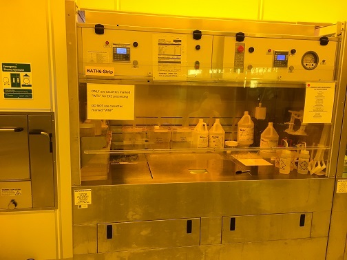
Solvent Bench
| Coral ID: | WNF--BATH6-Strip |
| Manufacturer: | WAFAB |
| Model: | 72" SST Front Acess |
| Lab: | WNF |
| Area: | Lithography and Direct Patterning |
| Manual: | https://www.coral.washington.edu/upload/manuals/BATH6-Strip_2.0.pdf |
Description
Solvent bench with an EKC photoresist stripping bath and a sonicator for liftoff processing.
Details
Refilled weekly
Materials Restrictions
(none)
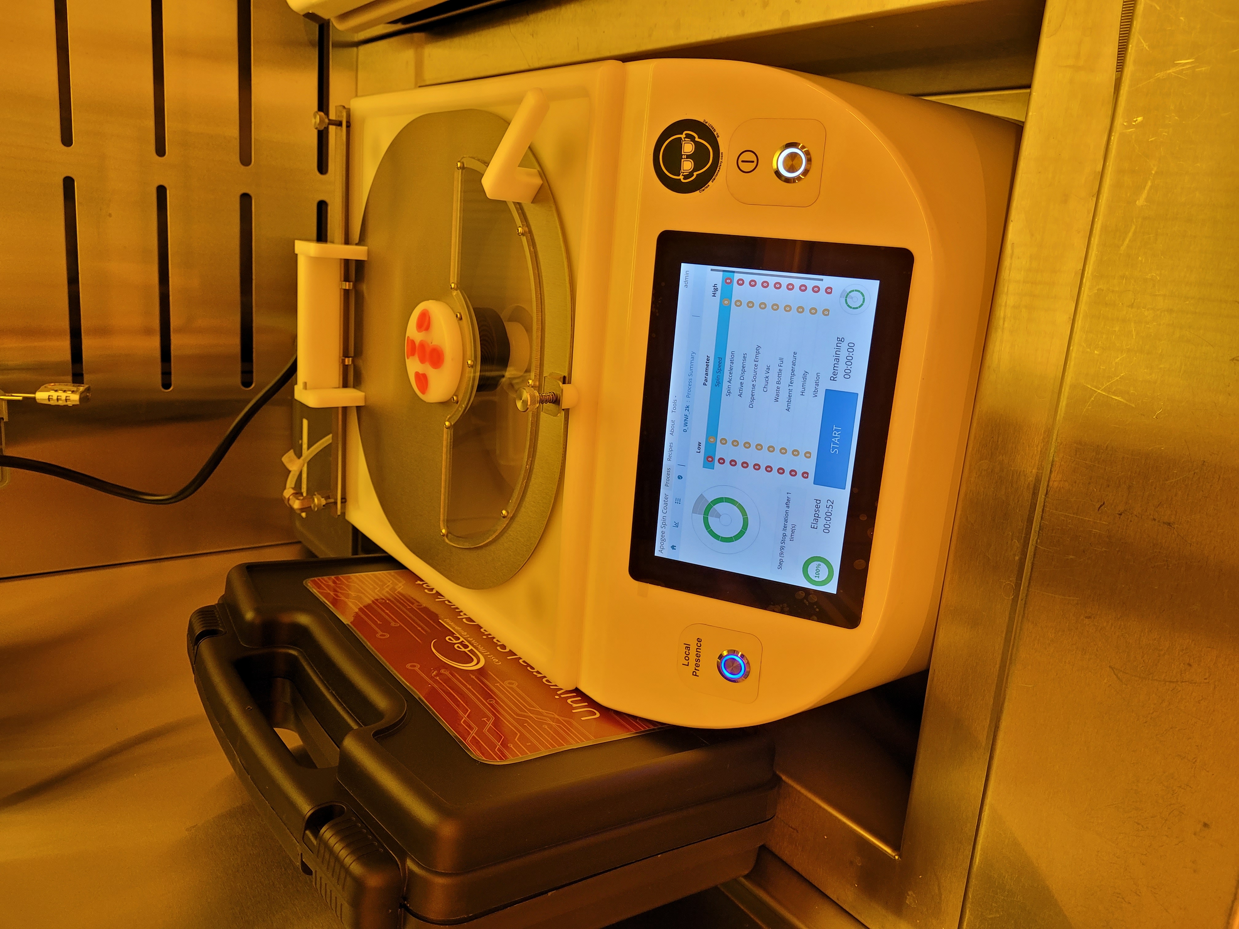
Spin Coater
| Coral ID: | WNF--SPIN3-EBeam |
| Manufacturer: | Cost Effective Equipment |
| Model: | APOGEE SPIN |
| Lab: | WNF |
| Area: | Lithography and Direct Patterning |
| Manual: | https://www.coral.washington.edu/upload/manuals/SPIN3_Apogee_SOP_V1.3.pdf |
| UW Academic Rate: | $55/hr |
| Industrial Rate: | $165/hr |
| Outside Academic Rate: | $55/hr |
Description
Manual, benchtop spin coater with vacuum chucking for samples from a few mm to 200mm wafers.
Details
(none given)
Materials Restrictions
Limited to use for Electron Beam Resists only!
Spin Coater
| Coral ID: | WNF--SPIN4-General |
| Manufacturer: | CEE |
| Model: | APOGEE SPIN |
| Lab: | WNF |
| Area: | Lithography and Direct Patterning |
| Manual: | https://www.coral.washington.edu/upload/manuals/SPIN4_5_Apogee_SOP_V1.2.pdf |
| UW Academic Rate: | $55/hr |
| Industrial Rate: | $165/hr |
| Outside Academic Rate: | $55/hr |
Description
Flexible, manual bench-top spin coater with vacuum chucks available for pieces from a few mm up to 200 mm wafers.
Details
(none given)
Materials Restrictions
(none)
.jpg)
Spin Rinse Dryer
| Coral ID: | WNF--SRD1-4in |
| Manufacturer: | Class One Technology |
| Model: | Avenger Ultra-Pure |
| Lab: | WNF |
| Area: | Wet Etch and Cleaning |
| Manual: | https://www.coral.washington.edu/upload/manuals/SRD SOP.pdf |
Description
4 inch Wafer Rinse / Dryer
Details
(none given)
Materials Restrictions
(none)
Spin Rinse Dryer
| Coral ID: | WNF--SRD1-6in |
| Manufacturer: | Class One Technology |
| Model: | Avenger Ultra-Pure |
| Lab: | WNF |
| Area: | Wet Etch and Cleaning |
| Manual: | https://www.coral.washington.edu/upload/manuals/SRD SOP.pdf |
Description
6 inch Wafer Rinse / Dryer
Details
(none given)
Materials Restrictions
(none)
SPTS PECVD
| Coral ID: | WNF--PECVD2-SPTS |
| Manufacturer: | SPTS |
| Model: | SPM |
| Lab: | WNF |
| Area: | Thin Film Processing |
| Manual: | https://www.coral.washington.edu/upload/manuals/PECVC2 SOP 20231130.pdf |
| UW Academic Rate: | $55/hr |
| Industrial Rate: | $165/hr |
| Outside Academic Rate: | $55/hr |
Description
Low temperature (125C) and high temperature (350C), high-rate PECVD of SiO, SiN, and amorphous-Si on up to 200mm substrates with dual frequency supplies for stress tuning.
Details
This system runs automated depositions by first conditioning the chamber, then running the deposition, and then cleaning. This makes the deposited films very repeatable and minimizes the need for systems shutdowns to clean the chamber.
Materials Restrictions
Because the system runs at high temperatures it is imperative that samples be compatible with those temperatures. Prior to deposition on low temperature materials or plastics, consult with staff.
SPTS Silicon DRIE
| Coral ID: | WNF--DRIE2--SPTS |
| Manufacturer: | SPTS |
| Model: | Rapier Si_DRIE |
| Lab: | WNF |
| Area: | Dry Etch |
| Manual: | https://www.coral.washington.edu/upload/manuals/SPTS-DRIE SOP v6.pdf |
| UW Academic Rate: | $77/hr |
| Industrial Rate: | $231/hr |
| Outside Academic Rate: | $77/hr |
Description
The SPTS Rapier is a highly functional inductively coupled ion etch tool that uses a time-multiplexed SF6-C4F8 process, also known as the Bosch Process. The parameter space for this tool is extensive and getting lost therein easily done. Several pseudo-standard recipes are available as starting points, but most processing on this tool will require some development. We're here to help.
Details
(none given)
Materials Restrictions
Etch target material is limited to silicon with mask material restricted to silicon oxide, silicon nitride, photoresist and e-beam resist. Wafer size is limited to 100mm only. It is not permitted to etch through wafer without a carrier or handle wafer between the etch target and the chuck. Note: No exposed metals (including copper, gold, and silver). Contact tool owner regarding restriction details.
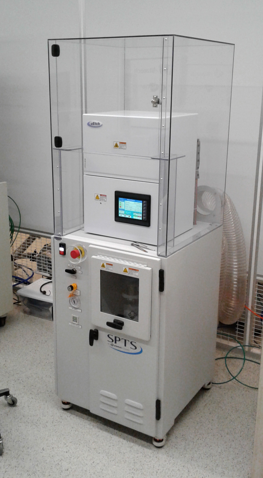
SPTS uEtch Module HF Vapor etcher
| Coral ID: | WNF--Vapor-Etch--HF |
| Manufacturer: | SPTS |
| Model: | MicroEtch |
| Lab: | WNF |
| Area: | Dry Etch |
| Manual: | https://www.coral.washington.edu/upload/manuals/HFVapor-Etch_v1.3b.pdf |
| UW Academic Rate: | $77/hr |
| Industrial Rate: | $231/hr |
| Outside Academic Rate: | $77/hr |
Description
This HF Vapor Dry Etch system is configured with Hydrofluoric and Ethanol vapor used, primarily, for isotropic etching of silicon dioxide without a plasma. The HFVapor system etches at reduced pressure and 45C to isotropically etch sacrificial silicon oxide layers, primarily to release silicon microstructures in MEMS devices. The dry process avoids stiction of released moving parts and damage to delicate structures – common issues with conventional wet processing technology. This is a single wafer system for 4 inch to 8 inch wafers and dies on a carrier wafer.
Details
Etch target is primarily silicon dioxide. Recommended mask materials are silicon, Al, Au, Cr, Ni, SiC, Al2O3, LPCVD nitride. PECVD nitride is NOT recommended as a masking material.
Materials Restrictions
POLYMERS INCLUDING PHOTO/EBEAM RESIST ARE NOT ALLOWED IN THIS SYSTEM. No polymers (including photo nor ebeam resists), no Kapton tape is allowed in the tool. Additional materials NOT ALLOWED: doped oxide, doped glass, borosilicate glass, soda-lime glass, float-glass, pyrex, Ti, TiO2, and copper. Do not use materials other than those known as approved. If a material that is not listed here, please contact the tool owner.
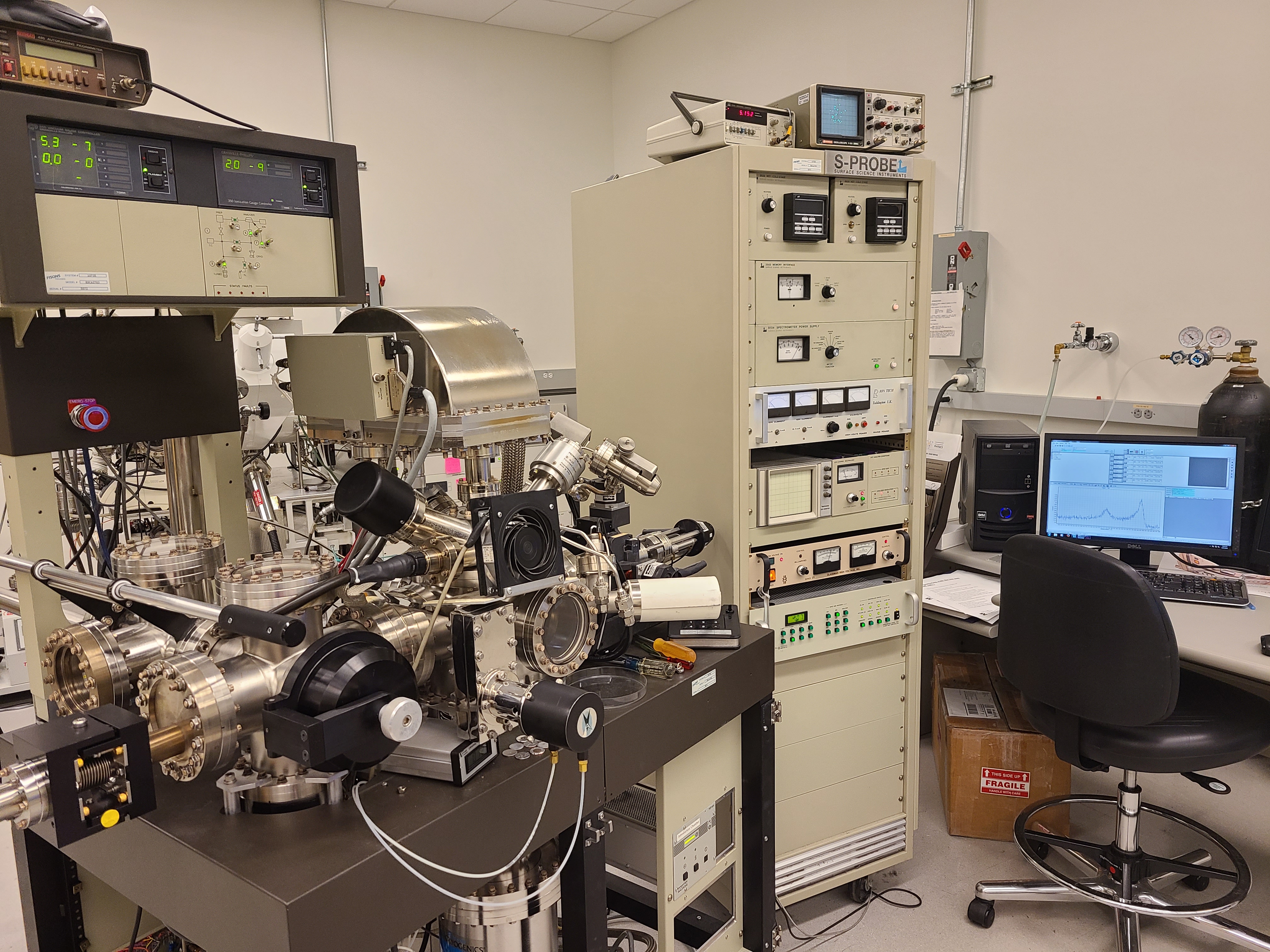
Surface Science Instruments S-Probe X-ray Photoelectron Spectrometer
| Coral ID: | SARC--S-Probe |
| Manufacturer: | Surface Science Instruments |
| Model: | S-Probe |
| Lab: | MAF |
| Area: | Thin Film and Materials Characterization |
| UW Academic Rate: | $48/hr |
| Industrial Rate: | $248/hr |
| Outside Academic Rate: | $58/hr |
Description
X-ray Photoelectron Spectroscopy (XPS) (which is also known as ESCA) exploits the photoelectric effect to obtain information about the chemical composition of a surface. XPS can identify all elements (except H and He) present in the outermost 10 nm of a surface that are in concentrations greater than 0.1 atomic %. The elemental composition of a surface can be quantified (±10% or better). High-resolution XPS spectra can provide information about the molecular environment of a particular element (oxidation state, bonding atoms, etc.) Since the major components of the XPS systems are under computer control, automated data acquisition is possible allowing the instrument to be used 24/7.
Details
The S-Probe is equipped with a monochromatic Al Kα x-ray source. The typical x-ray spot size used for analysis is 800 microns, but smaller spot size analysis is possible down to 50 microns. Samples up to 3x3 cm can be measured.
Materials Restrictions
(none)
Suss Spin Coater
| Coral ID: | WNF--SPIN2 |
| Manufacturer: | Suss Microtec |
| Model: | LabSpin8 |
| Lab: | WNF |
| Area: | Lithography and Direct Patterning |
| Manual: | https://www.coral.washington.edu/upload/manuals/SPIN1_2_SOP_2022.pdf |
| UW Academic Rate: | $55/hr |
| Industrial Rate: | $165/hr |
| Outside Academic Rate: | $55/hr |
Description
Spin 100-200mm wafers, with a programmable controller, in a class 10 mini-environment, and a dedicated, electro-polished hotplate with automated wafer lift pins.
Details
(none given)
Materials Restrictions
(none)
Suss Spin Coater
| Coral ID: | WNF--SPIN1 |
| Manufacturer: | Suss Microtec |
| Model: | LabSpin8 |
| Lab: | WNF |
| Area: | Lithography and Direct Patterning |
| Manual: | https://www.coral.washington.edu/upload/manuals/SPIN1_2_SOP_2022.pdf |
| UW Academic Rate: | $55/hr |
| Industrial Rate: | $165/hr |
| Outside Academic Rate: | $55/hr |
Description
Spin 100-200mm wafers, with a programmable controller, in a class 10 mini-environment, and a dedicated, electro-polished hotplate with automated wafer lift pins.
Details
(none given)
Materials Restrictions
(none)
Tecnai G2 F20 SuperTwin
| Coral ID: | MAF--TEM--FEI-Tecnai |
| Manufacturer: | FEI |
| Model: | Tecnai G2 F20 SuperTwin |
| Lab: | MAF |
| Area: | Inspection |
| UW Academic Rate: | $80/hr |
| Industrial Rate: | $286/hr |
| Outside Academic Rate: | $93/hr |
Description
200 kV HR transmission electron microscope with DF scanning capabilities (S/TEM), EDAX Elite-T EDS, diffraction, and tomography. Supplied with a Gatan Ultrascan CCD digital camera. Point to point resolution is 0.24 nm with information limit of 0.102 nm.
Details
Contact Ellen Lavoie at lavoie@uw.edu for training or questions.
Materials Restrictions
Discuss with TEM manager
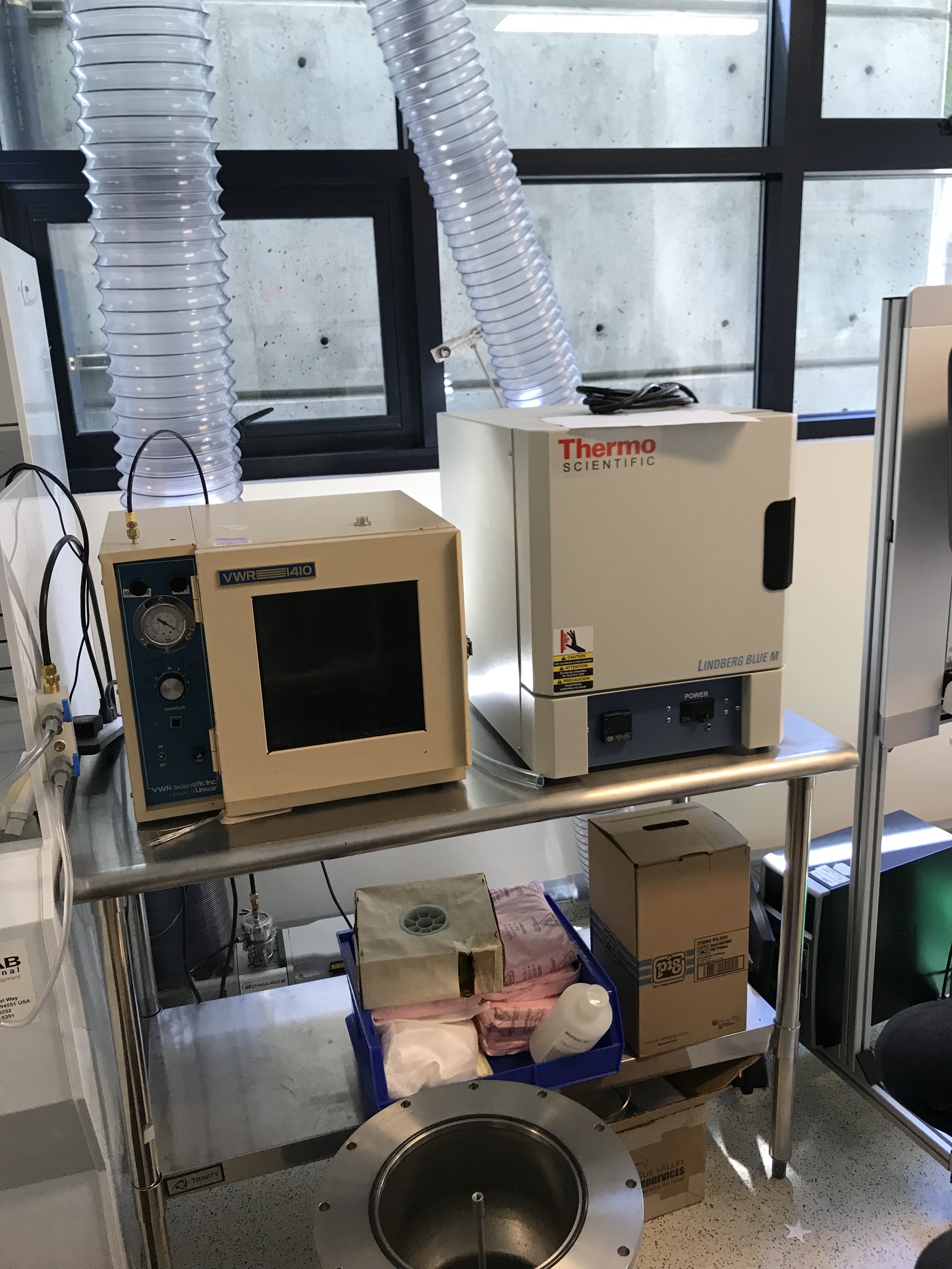
Thinky Mixer
| Coral ID: | WNF--Thinky-Mixer |
| Manufacturer: | Thinky |
| Lab: | WNF |
| Area: | Lithography and Direct Patterning |
| UW Academic Rate: | $11/hr |
| Industrial Rate: | $33/hr |
| Outside Academic Rate: | $11/hr |
Description
The Thinky mixer is used to mix and degas PDMS.
Details
(none given)
Materials Restrictions
(none)
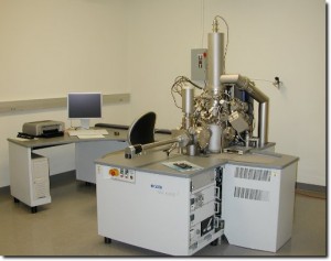
Time-of-flight secondary ion mass spectrometry
| Coral ID: | SARC--ION-TOF |
| Manufacturer: | IONTOF |
| Model: | TOF.SIMS 5 |
| Lab: | MAF |
| Area: | Thin Film and Materials Characterization |
| UW Academic Rate: | $90/hr |
| Industrial Rate: | $225/hr |
| Outside Academic Rate: | $100/hr |
Description
ToF-SIMS is a surface analytical method that provides chemically specific information about the upper 1-2 nm of a surface. The IONTOF TOF.SIMS 5 is capable of producing high mass resolution spectra (m/detlaM ~ 6000-10000) and high spatial resolution images (< 1 micron edge resolution) of any surface that can be placed in an ultra high vacuum environment. The TOF.SIMS 5 also has a gas cluster ion beam (GCIB) for sputtering which enables depth profiling of organic materials.
Details
The SIMS process is initiated by bombarding the surface of a solid sample with an energetic beam of ions (1-50 keV). This primary ion beam bombardment results in the ejection of atoms and molecular fragments from the surface region. Only a small percentage of the emitted fragments are positive or negative ions. It is these secondary ions that are mass analyzed in SIMS. In static mode of ToF SIMS, the primary ion beam is maintained at a very low fluence (typically less than 1012 ions/cm2) so that secondary ions are not emitted from an area damaged previously by another primary ion, resulting in the emission of molecular fragments from organic and biological materials. The structure and composition of these fragments is directly related to the molecular structure of the surface they were emitted from. Thus, analysis of the type and amounts of secondary ions emitted from a sample under static SIMS conditions provides information about the molecular surface structure of organic and biological materials. When used in conjunction with other surface sensitive techniques such as electron spectroscopy for chemical analysis (ESCA), a detailed understanding of surface structure and composition can be obtained.
A key feature of modern, state-of-the-art SIMS systems is the ToF analyzer used to detect the secondary ions. The ions are extracted from the sample and accelerated into the field-free analyzer with a common energy (but different velocities). The difference in velocities means the smaller ions move through the analyzer more rapidly than the larger ions, providing mass separation of the ions. When the secondary ions strike the detector their masses are determined from the time it took them to travel through the analyzer. Overall, the combination of the ToF analyzer with the static SIMS process results in a powerful surface analysis technique.
ToF-SIMS Capabilities:
- A mass spectrum of the outermost 15Å of a surface
- Identification of structural units present at the surface, e.g. monomeric components and repeat units)
- Fingerprint identification of polymers
- Information on surface degradation and contamination
- Spatial imaging of the surface chemistry
Information provided by ToF-SIMS:
- Molecular conformation
- Molecular orientation
- Molecular mobility
- Sample damage
- Extent of crosslinking
- Molecular interactions
- Assembly orientation and perfection
- Quantitation
ToF-SIMS Applications:
- Detection of contaminants
- Identification of surface-active additives
- Characterization of surface modification treatments
- Examination of adsorbed/immobilized biomolecules
- Determination of supramolecular structures
- Chemical imaging of patterned surfaces
Special ToF-SIMS capabilities at our facility:
- Frozen-hydrated analysis (“cold stage”)
- Multiple sample handling
- Depth profiles of organic materials
- Variable temperature analysis
Materials Restrictions
All samples must be vacuum compatible. Samples containing PDMS are not allowed unless specific permission is obtained prior to analysis. An extra fee will be charged for analysis of PDMS materials to cover cleaning and checking of the system.
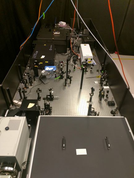
Transient Absorption-Time Resolved Photoluminescence
| Coral ID: | MAF--Laser--TA-TRPL |
| Manufacturer: | Coherent/Ultrafast Systems/Hammamatsu |
| Model: | Libra/Opera-Topas/Helios-Eos |
| Lab: | MAF |
| Area: | Other |
| UW Academic Rate: | $34/hr |
| Industrial Rate: | $126/hr |
| Outside Academic Rate: | $40/hr |
Description
Femtosecond laser system with transient absorption and streak camera detectors capable of measuring photoexcited spectra, photoluminescence, and kinetics of thin film and solution phase samples.
Details
The output of the Libra (800 nm, 1 kHz, 40 fs) has the capability to pump 1 or 2 OPAs with outputs ranging from the UV to IR, as well as generate a broadband probe from the UV to NIR. The Helios system allows for transient absorption detection in the fs-ns range, while the EOS system extends from the ns-ms range. Streak camera allows for detection of photoluminescence in the ps-ms time range.
Materials Restrictions
(none)
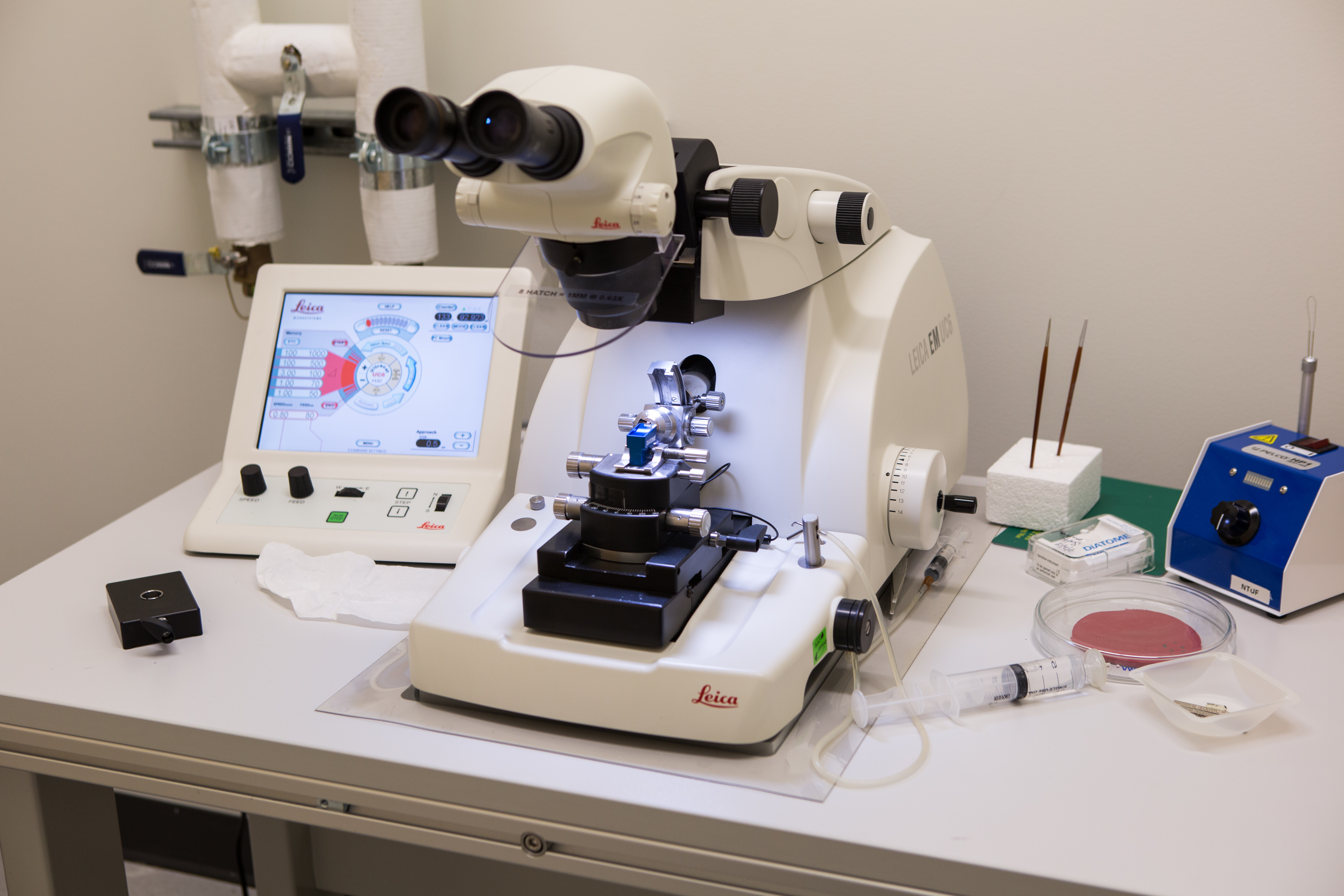
Ultracut 6 Microtome
| Coral ID: | MAF--Microtome--Leica-UC-6 |
| Manufacturer: | Leica |
| Model: | UC-6 |
| Lab: | MAF |
| UW Academic Rate: | $34/hr |
| Industrial Rate: | $126/hr |
| Outside Academic Rate: | $40/hr |
Description
Automatic cutting microtome for either wet or dry sectioning of 20 nm-several microns.
Details
Full training including preparation of samples and use of diamond knife for ultrathin sectioning samples is offered.
Materials Restrictions
No lead; discuss samples with staff
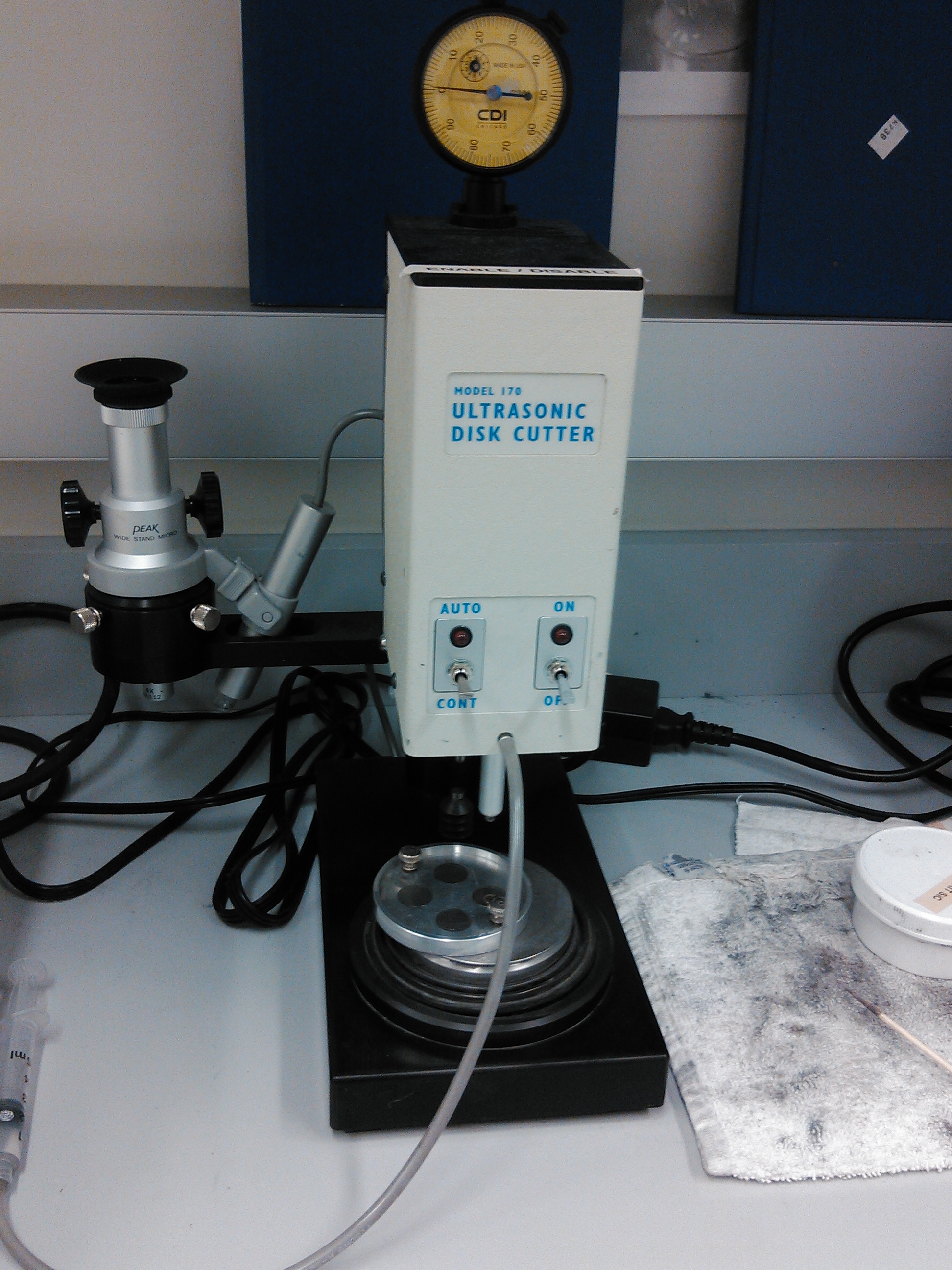
Ultrasonic Disc Cutter
| Coral ID: | MAF--Disc-Cutter--Fischione-170 |
| Manufacturer: | Fischione |
| Model: | 170 |
| Lab: | MAF |
| UW Academic Rate: | $34/hr |
| Industrial Rate: | $126/hr |
| Outside Academic Rate: | $40/hr |
Description
Ultrasonically cut various size/shape discs for preparation of samples for TEM.
Details
(none given)
Materials Restrictions
Must contact staff for training and qualification.
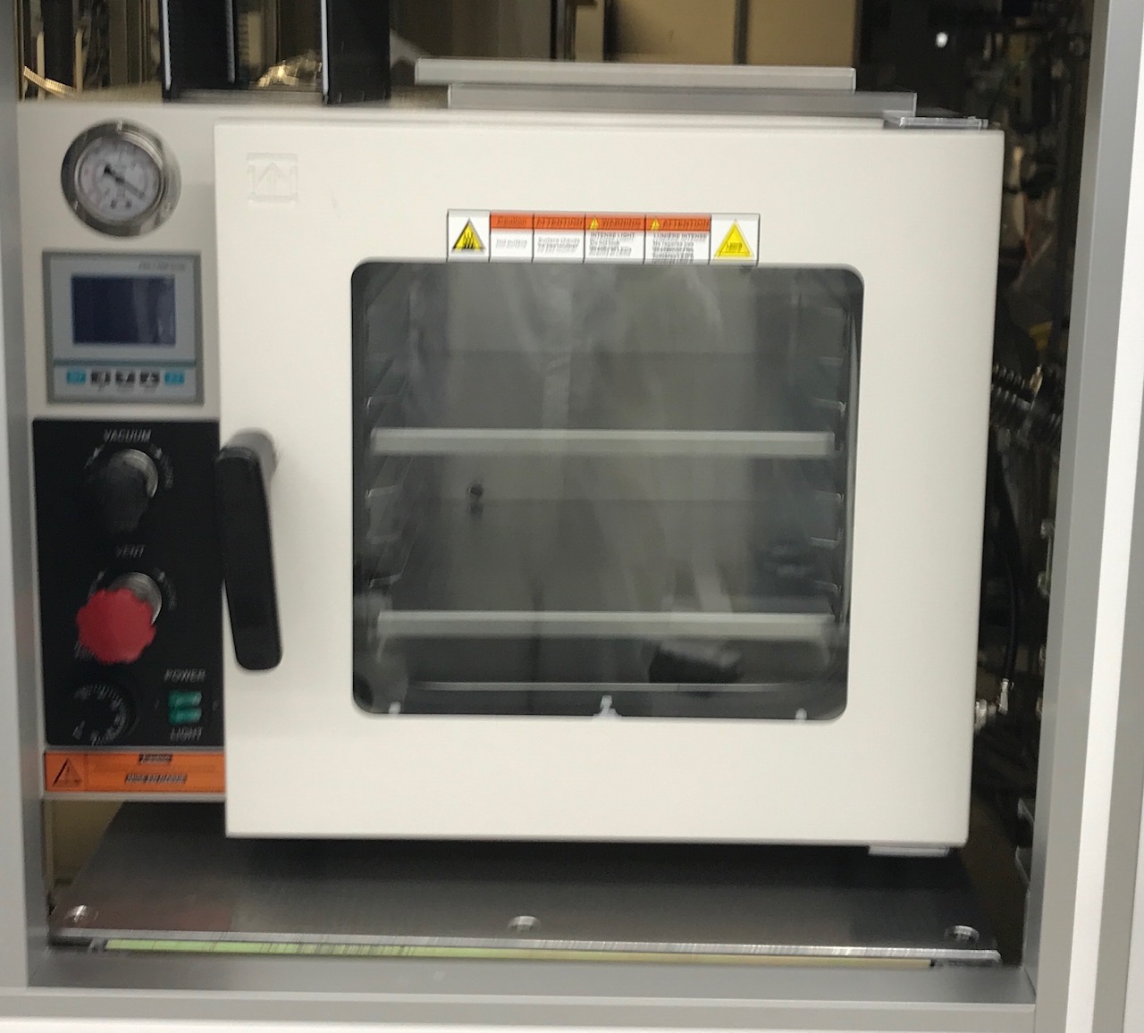
Vacuum Oven
| Coral ID: | WNF--VacOven--Accutemp |
| Manufacturer: | Across International |
| Model: | ACCUTEMP-09 |
| Lab: | WNF |
| Area: | Lithography and Direct Patterning |
| UW Academic Rate: | $11/hr |
| Industrial Rate: | $33/hr |
| Outside Academic Rate: | $11/hr |
Description
Programmable vacuum oven with N2 backfill capability.
Details
Vacuum levels ranging from 1atm to ~0.5torr and equipped with an N2 backfill capability for inert environment. Operating temperature up to 250C, accuracy within +/- 1C. Can be programmed to automatically control a multi-segment drying process.
Materials Restrictions
(none)
.jpg)
Wafer Cleaver
| Coral ID: | WNF--Cleaver--LatticeGear-AX420 |
| Manufacturer: | LatticeGear |
| Model: | AX420 |
| Lab: | WNF |
| Area: | Packaging and Back End |
| Manual: | https://www.coral.washington.edu/upload/manuals/Cleaver - LatticeGear AX420 SOP 20180328.pdf |
| UW Academic Rate: | $33/hr |
| Industrial Rate: | $99/hr |
| Outside Academic Rate: | $33/hr |
Description
Precision diamond indentation and break station
Details
(none given)
Materials Restrictions
Recommended for single crystal semiconductor wafers
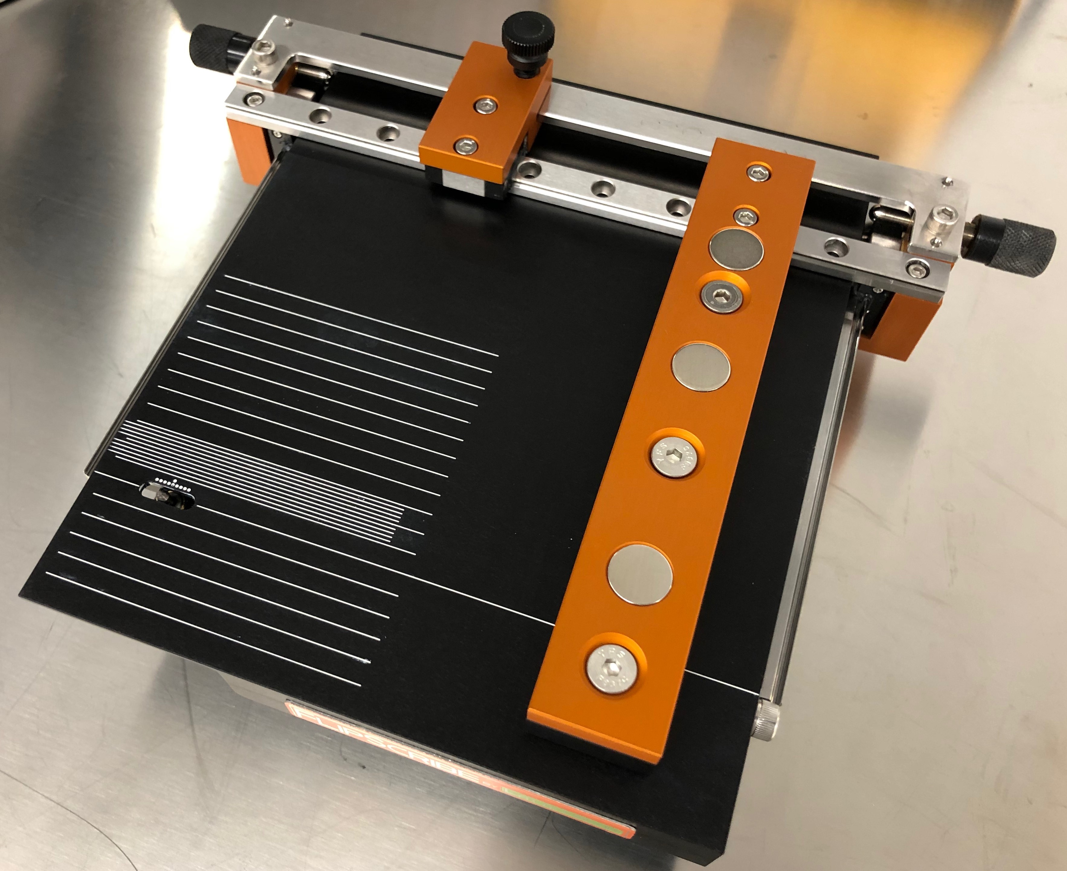
Wafer Scriber
| Coral ID: | WNF--Scriber--LatticeGear-FlipScribe |
| Manufacturer: | LatticeGear |
| Model: | FlipScribe |
| Lab: | WNF |
| Area: | Other |
| UW Academic Rate: | $0/hr |
| Industrial Rate: | $0/hr |
| Outside Academic Rate: | $0/hr |
Description
Manual scribing fixture for full and partial wafers, specifically designed for scribing the back side of the sample. Scribes across full wafers are possible, which is especially helpful for glass.
Details
4" wafer and small sample holders are available. Others are possible to obtain, please discuss specific needs with staff.
Materials Restrictions
Glass, sapphire, semiconductors. Dry samples only.
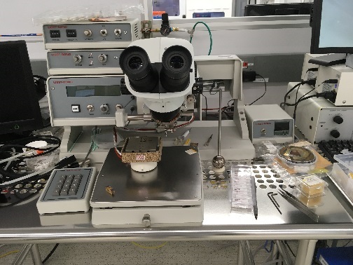
WEST-BOND Wire Bonder
| Coral ID: | WNF--WestBond |
| Manufacturer: | WestBond |
| Model: | 4700E |
| Lab: | WNF |
| Area: | Packaging and Back End |
| Manual: | https://www.coral.washington.edu/upload/manuals/Westbond wirebonder SOP 2.1 - CURRENT.pdf |
| UW Academic Rate: | $55/hr |
| Industrial Rate: | $165/hr |
| Outside Academic Rate: | $55/hr |
Description
Wire bonding is used to electrically connect semiconductor devices with their packaging. The Westbond 4700E is a semiautomatic thermosonic ball-wedge wire bonder. It can be used to quickly lay down a succession of shaped electrical interconnects, or simple stud bumps for bonding chips using the flip chipper. The shaping and bonding of the wire is automated while the X-Y placement is manual, making it ideal for quickly generating testable prototypes and small batches of working devices. The wire is 1 mil (25um) gold wire.
Details
(none given)
Materials Restrictions
(none)
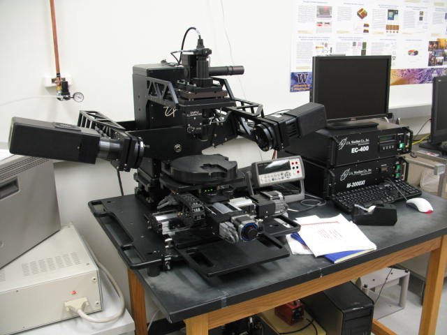
Woollam Spectroscopic Ellipsometer
| Coral ID: | MAF--Ellipsometer--Woollam-M-2000 |
| Manufacturer: | Woollam |
| Model: | M-2000 |
| Lab: | MAF |
| Area: | Thin Film and Materials Characterization |
| Manual: | https://www.coral.washington.edu/upload/manuals/Woollam Ellipsometer SOP_150311.docx |
| UW Academic Rate: | $34/hr |
| Industrial Rate: | $126/hr |
| Outside Academic Rate: | $40/hr |
Description
Used for determination of thicknesses and optical parameters of thin films and multilayers; Spectral range: 210-1700nm; Spot size: normal > 1.5 mm, focused <150 μm; Sample mapping; Heating option: to 300 °C
Details
(none given)
Materials Restrictions
(none)
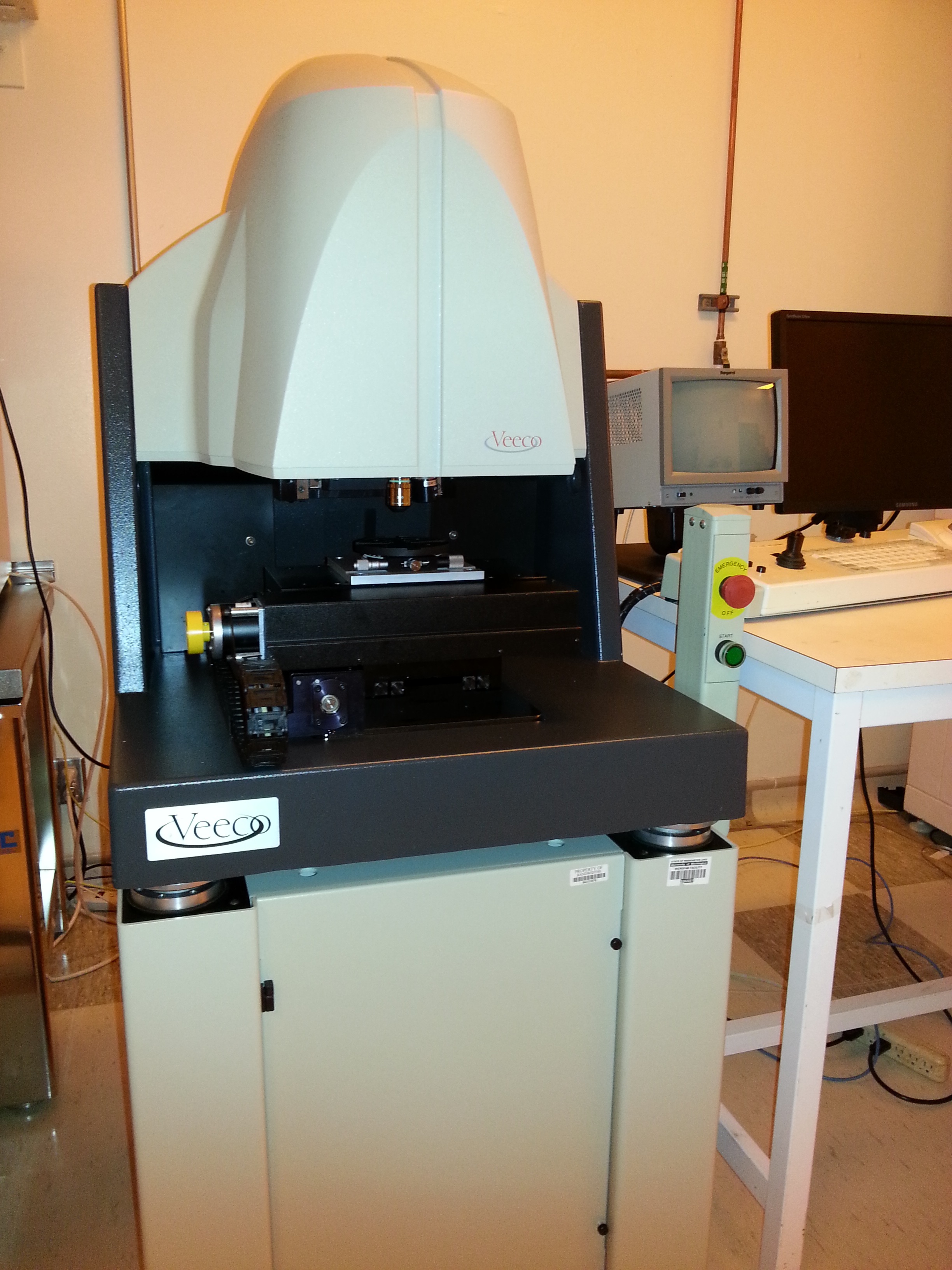
Wyko NT3300
| Coral ID: | WNF--Profilometer--Wyko |
| Manufacturer: | Veeco |
| Model: | Wyko NT3300 |
| Lab: | WNF |
| Area: | Device and Structure Characterization |
| Manual: | https://www.coral.washington.edu/upload/manuals/Wyko.pdf |
| UW Academic Rate: | $55/hr |
| Industrial Rate: | $165/hr |
| Outside Academic Rate: | $55/hr |
Description
This instrument takes non-contact 3D surface topography measurements using optical interference. Single nanometer resolution is possible using both phase-shifting interferometry and vertical scanning interferometry. The stage is set up for samples up to 100 mm. The tool is capable of stitching and automated sequences.
Details
(none given)
Materials Restrictions
(none)
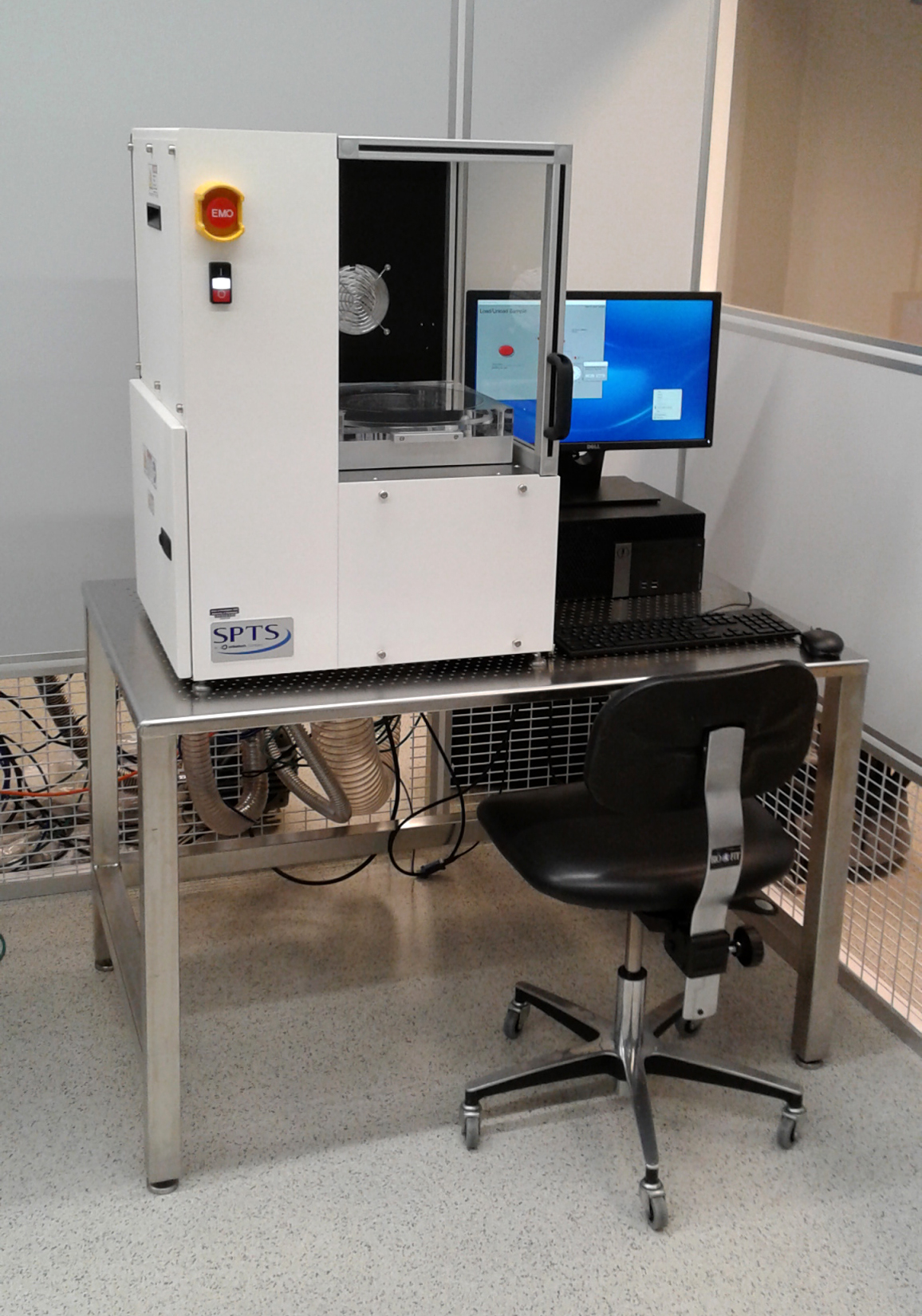
Xenon Difluoride vapor etcher
| Coral ID: | WNF--Vapor-Etch--XeF2 |
| Manufacturer: | SPTS |
| Model: | e2 |
| Lab: | WNF |
| Area: | Dry Etch |
| Manual: | https://www.coral.washington.edu/upload/manuals/XeF2Vapor-Etch_v1.2.pdf |
| UW Academic Rate: | $77/hr |
| Industrial Rate: | $231/hr |
| Outside Academic Rate: | $77/hr |
Description
The XeF2 vapor etch tool is for primarily for isotropic chemical etching of silicon sacrificial layers for the release of MEMS structures.
Details
Xenon difluoride (XeF2) provides a highly selective isotropic etch for Si, Mo and Ge and is an ideal solution for etching sacrificial layers to “release” moving components within MEMS devices. It provides numerous unique advantages and capabilities compared to wet and SF6 plasma etch options. The process is generally carried out at pressures between 0.5 and 4 torr providing controlled, stiction-free and residue-free etching. Typical vertical and lateral silicon etch rates are in the 0.1 - 10 microns/minute range. Because of its selectivity and excellent reach, XeF2 can be used to make very long undercuts with little or no degradation of etch stop, mask or device layers. Silicon dioxide masks, with a Si:oxide selectivity of >1,000:1, have been used to achieve very long undercuts (well over 100μm) and to protect extremely small or thin devices (less than 30nm). XeF2 does not attack polymers or other organic films. Photoresist can be used as a cost-effective mask and polymeric passivation layers, such as those from the Bosch Process, can be used as an effective protective layer for trench sidewalls. XeF2 is also an ideal way to release PDMS, parylene, and SU8. Since XeF2 does not etch packing and dicing materials, it can increase yield by delaying the release of a MEMS device until after dicing or package insertion and wire bonding. XeF2 has been used successfully to release MEMS devices on diced wafers and chips inside packages.
Materials Restrictions
Allowed etch target materials: silicon, germanium, molybdenum, SiGe, Ti, W. Allowed masks(typical selectivity): photo/ebeam resists, PDMS, silicon dioxide(1000:1), silicon nitride(100:1), Au, Al, Ni, Cr, Pt, SiC. DO NOT use this tool for thinning silicon wafers or to thin silicon chips. See tool owner for further information.
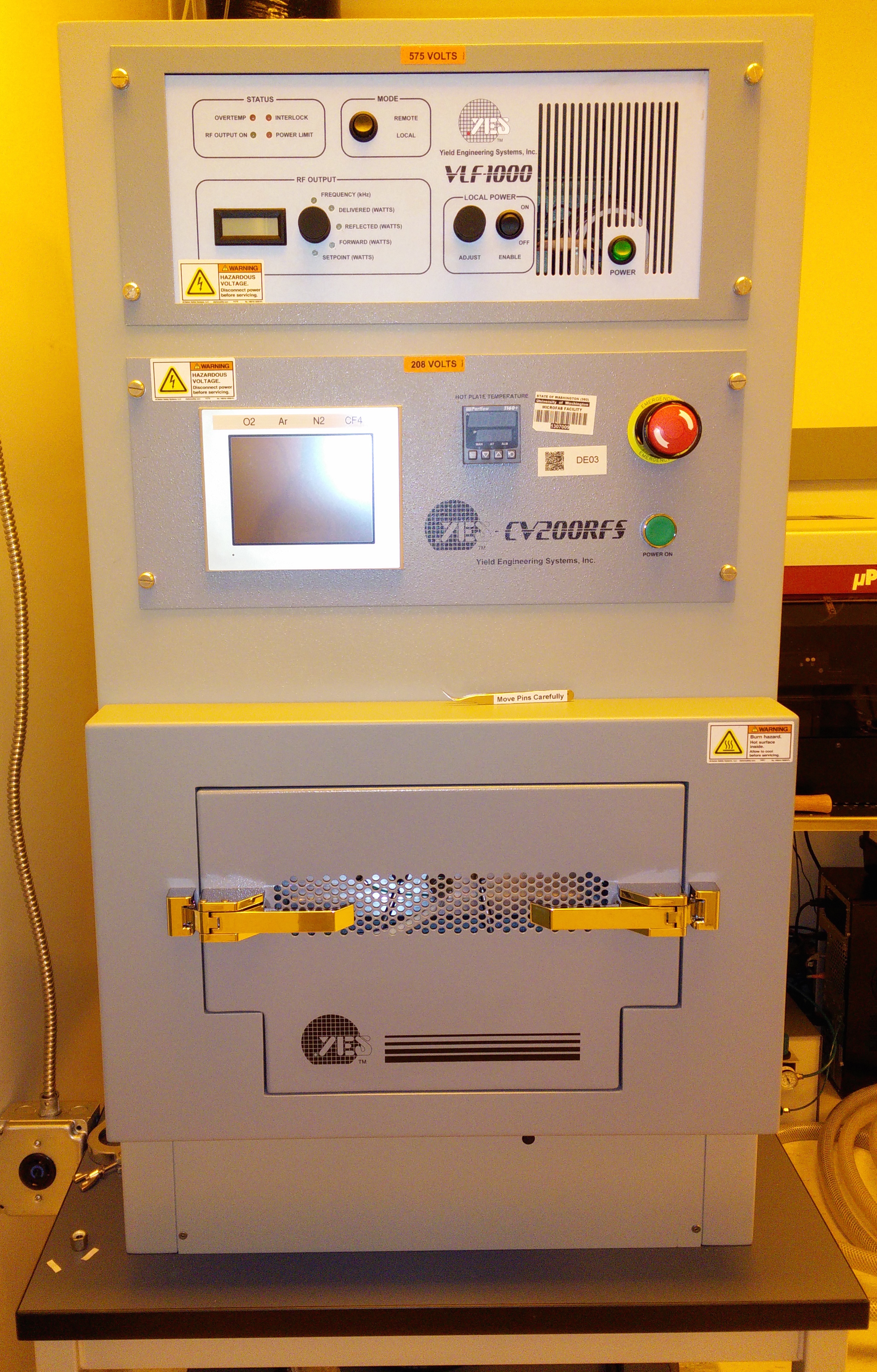
YES Downstream Asher
| Coral ID: | WNF--Etcher--Yes-Asher |
| Manufacturer: | Yield Engineering Systems (YES) |
| Model: | YES CV200 RFS |
| Lab: | WNF |
| Area: | Lithography and Direct Patterning |
| Manual: | https://www.coral.washington.edu/upload/manuals/ASH2-YES_UserManual_v3c.pdf |
| UW Academic Rate: | $77/hr |
| Industrial Rate: | $231/hr |
| Outside Academic Rate: | $77/hr |
Description
Downstream asher used to remove organics from various materials. Available process gases: O2, Argon, N2
Details
A heated, tray-load system, the YES Downstream Asher offers a high degree of process control with 3 available process gases. The tool has 4 standard recipes for thin film resist stripping, thick film resist stripping, and substrate descum. Users are requested to work with the tool owner to develop process specific recipes.
Materials Restrictions
Allowed etch target materials: Photoresist, e-beam resist, organic contaminants, some polymers (No SU8 nor PDMS.) No high-vapor-pressure materials. Please contact tool owner to discuss materials not included on this list.
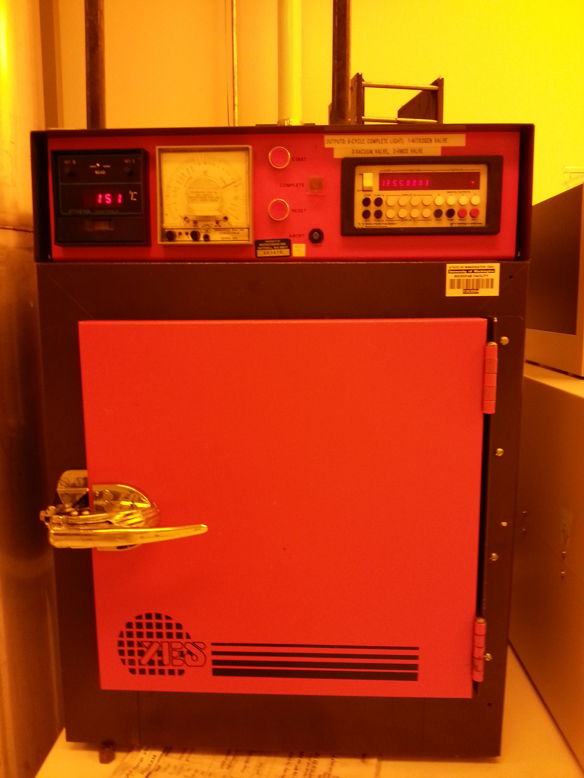
YES HMDS Oven
| Coral ID: | WNF--HMDS |
| Manufacturer: | Yeild Enginerring Systems |
| Model: | LP 3 A |
| Lab: | WNF |
| Area: | Lithography and Direct Patterning |
| Manual: | https://www.coral.washington.edu/upload/manuals/HMDS_SOP_20211111.pdf |
| UW Academic Rate: | $33/hr |
| Industrial Rate: | $99/hr |
| Outside Academic Rate: | $33/hr |
Description
HMDS oven used for priming wafers prior to resist coating
Details
(none given)
Materials Restrictions
(none)
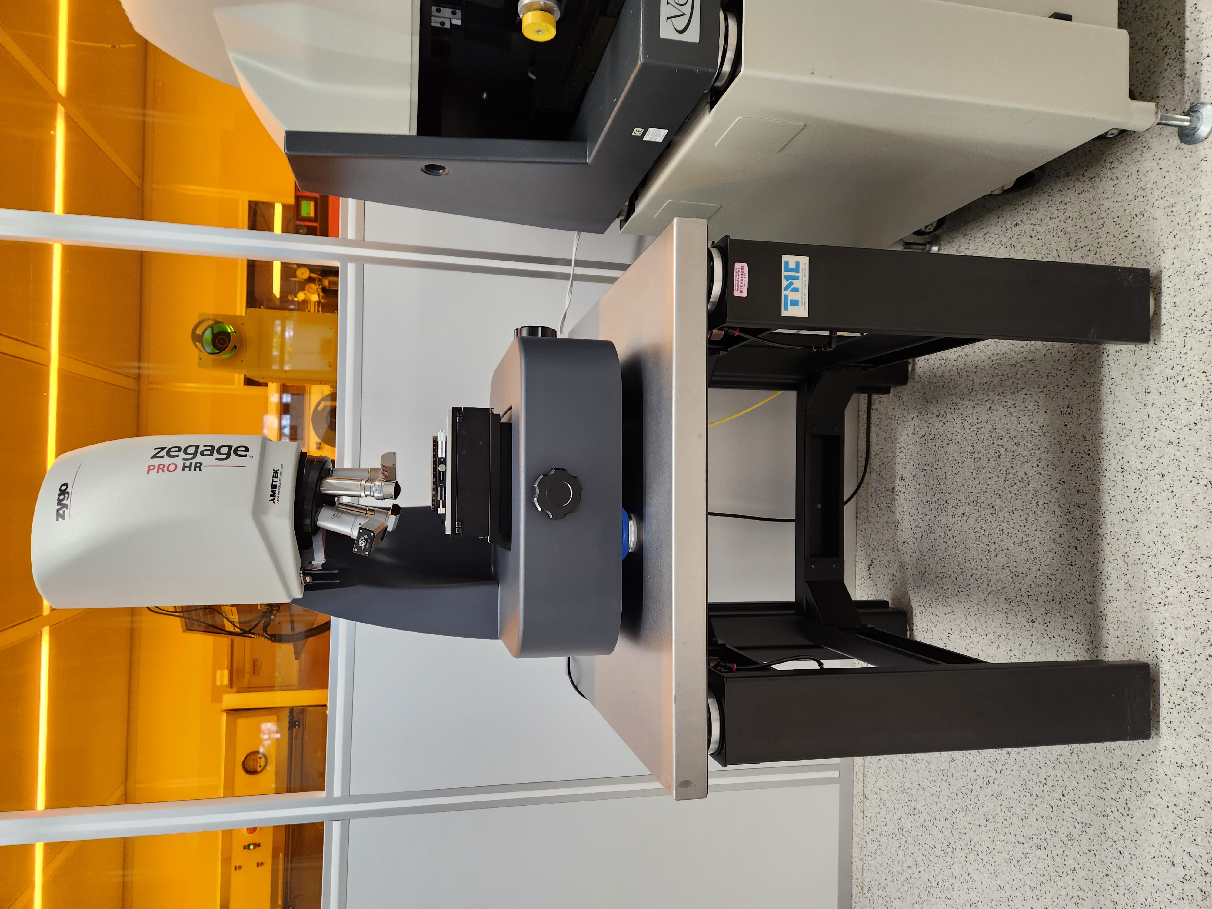
Zygo ZeGage Pro HR
| Coral ID: | WNF--Profilometer--Zygo-ZeGage-Pro-HR |
| Manufacturer: | Zygo |
| Model: | ZeGage Pro HR |
| Lab: | WNF |
| Area: | Device and Structure Characterization |
| Manual: | https://www.coral.washington.edu/upload/manuals/SOP Draft Zygo.pdf |
| UW Academic Rate: | $55/hr |
| Industrial Rate: | $165/hr |
| Outside Academic Rate: | $55/hr |
Description
The ZeGage Pro HR is a high resolution 3D optical profilometer using white light interferometry to achieve sub-nanometer resolution.
Details
Specifications:
Vertical scan range: 20 mm
Surface topography repeatability: ≤ 0.15 nm
Repeatability of RMS: 0.01 nm
Step height accuracy: ≤ 3%
Features include:
- Objectives:
- Measurement array up to 1600x1200
- Motorized stage and automation with 100 mm travel
Materials Restrictions
Samples must be clean and dry. No residue should be left behind on the stage.